
Simple FM transmitter circuit
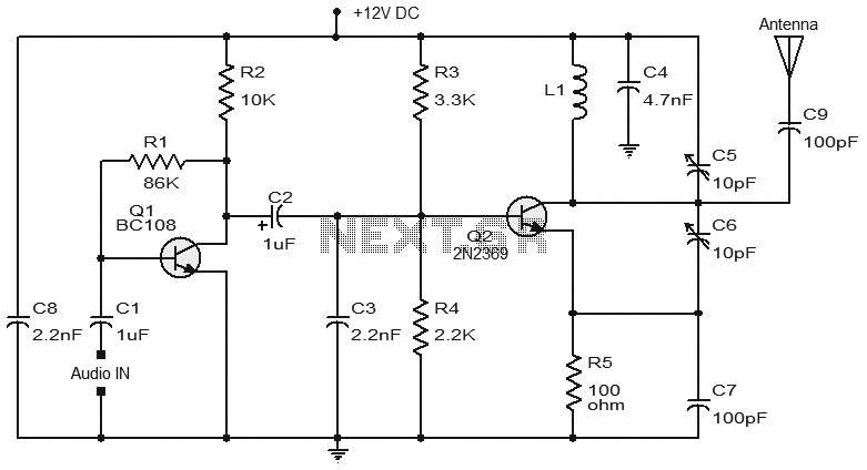
The described FM transmitter circuit is a straightforward design that utilizes two transistors to achieve modulation and amplification of audio signals for FM transmission. The preamplifier stage, utilizing transistor Q1, is critical for amplifying the input audio signal before it is processed further. The collector-to-base configuration allows for stable operation, with R1 and R2 carefully selected to ensure optimal biasing and collector current levels, thereby maximizing the performance of the amplifier.
The coupling capacitor C1 is essential for blocking any DC component of the audio signal, allowing only the AC audio signal to pass through to the base of Q1. This ensures that the transistor operates within its linear region, providing a clean amplification of the audio input.
Following the preamplifier, the oscillator and modulator stage, built around transistor Q2, plays a key role in generating the FM signal. The coupling capacitor C2 connects the amplified audio signal from Q1 to the base of Q2, where it modulates the oscillation frequency. Resistors R3 and R4 are critical for establishing the proper biasing conditions for Q2, ensuring reliable operation in the active region.
The inclusion of the emitter resistor R5 stabilizes the operating point of Q2 and improves linearity, which is crucial for maintaining signal integrity during modulation. The tank circuit, composed of inductor L1 and the trimmer capacitor C5, is vital for generating oscillations at the desired frequency. The trimmer capacitor allows for fine-tuning of the oscillator frequency, enabling the transmitter to operate at a specific FM band frequency.
Finally, the modulated FM signal is made available at the collector of Q2. Capacitor C9 facilitates the coupling of this signal to the antenna, allowing for efficient transmission of the FM signal over the airwaves. Overall, this simple two-transistor FM transmitter circuit exemplifies a fundamental approach to FM transmission, suitable for various applications in amateur radio and educational projects.A lot of FM transmitter circuits have been already published here. This just another one, a simple two transistor FM transmitter. The first stage of the circuit is a preamplifier stage based on transistor Q1. This is a collector to base biased amplifier stage where resistor R2 sets the collector current and R1 provided the necessary collector to ba se bias. C1 is the input DC decoupling capacitor which couples the input audio signal to the Q1 base. C8 is the power supply by-pass capacitor. Next stage is the oscillator cum modulator stage built around transistor Q2. Electrolytic capacitor C2 couples the output of the first stage to the second stage. R3 and R4 are the biasing resistors of Q2. R5 is the emitter resistor of Q2. Inductor L1 and trimmer capacitor C5 forms the tank circuit which is necessary for creating oscillations. The modulated FM signal is available at the collector of Q2 and it is coupled to the antenna using capacitor C9.
🔗 External reference
Related Circuits
In these circuits, a set of switches (conforming to code) are pressed sequentially within a specified time to unlock the mechanism. In some configurations, custom-built integrated circuits (ICs) are utilized, and positive and negative logic pulses are input in...
Nowadays, an increasing number of audio-visual devices in homes are interconnected. This is particularly true for televisions, which may be linked to DVD players. In modern home entertainment systems, the integration of various audio-visual devices enhances user experience and convenience....
By adjusting the Adjust pin, the output voltage and current can be regulated. A variable resistor (VR) is connected between the Adjust pin and ground to achieve an output voltage of 9 volts to the battery. Resistor R3 limits...

This circuit utilizes a JFET to receive signals from an LED and buffer them. The output voltage is managed using an IC 1458 or LM1458, which provides approximately 7 volts in darkness and experiences a drop of about 2...
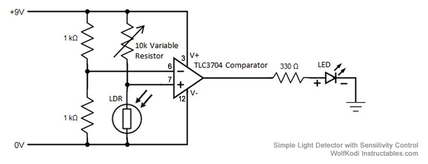
The schematic diagram for the circuit is provided in the accompanying image. As indicated by its name, a comparator is designed to compare two specified voltages. The circuit includes a pair of 1K resistors. A comparator circuit typically utilizes operational...
The telephone line tester comprises a meter used to measure line voltage in both the on-hook and off-hook states, three resistors (including one variable resistor), a pushbutton switch, and a modular telephone connector. When the circuit is connected to...
Warning: include(partials/cookie-banner.php): Failed to open stream: Permission denied in /var/www/html/nextgr/view-circuit.php on line 713
Warning: include(): Failed opening 'partials/cookie-banner.php' for inclusion (include_path='.:/usr/share/php') in /var/www/html/nextgr/view-circuit.php on line 713