
Simple Power Down Circuit Circuit
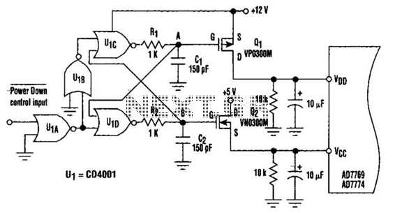
Specifically, raising the power-down control causes the output of U1C to go low, resulting in capacitor C1 discharging exponentially with a time constant. As the voltage on C1 decreases, two key events occur. First, this creates a negative gate-source voltage on the P-channel MOSFET Q1, turning it on. Second, this action drives the output of U1D high. With U1D's output high, capacitor C2 charges exponentially to approximately 12 V, applying a positive gate-source voltage that turns on Q2. In the power-down mode, when the power-down control is set low, the RC circuits and their associated delays operate in reverse. Consequently, capacitor C2 discharges to the logic input of U1C before C1 can charge, resulting in Q2 turning off before Q1.
This circuit is designed to effectively manage the power sequencing of analog I/O devices, ensuring that they remain protected from potential damage caused by improper power application. The use of MOSFETs for switching provides a low-resistance path when activated, minimizing power loss and improving efficiency. The cross-coupled NOR gates serve a critical role in controlling the timing of the power application and removal, thereby ensuring that the sequence is maintained within safe operational limits.
The power-down control mechanism is crucial for systems where power management is essential. By integrating this function, the circuit not only enhances the reliability of the connected devices but also simplifies the overall design by eliminating the need for additional protective diodes. The careful design of the RC timing networks ensures that the transition between power states is smooth, thus protecting sensitive components from voltage spikes and ensuring stable operation during power cycling. This circuit, adds a power-down function to analog I/O ports (for example, the AD7769 and AD7774). Moreover, the diodes ordinarily needed to protect the devices against power-supply mis-sequencing can be eliminated (see the figure).In the circuit, MOSFETs Ql and Q2 switch the +5- and +12-V supplies, respectively, in a sequence controlled by two cross-coupled CD4001 CMOS NOR gates (U1C and U1D). The sequence in which power is applied is important: The controlled circuits may be damaged anytime Vcc exceeds VDD + 0.3 V.
Consequently, the NOR gates must be powered from a 12-V supply throughout the power-down sequence.Bringing the power down control high (+5 V) applies power to the controlled circuit by turning on all MOSFETs. Specifically, raising the power down brings the output of U1C low, causing capacitor CI to discharge VOL exponentially with time constant0. As the voltage on CI falls, two events occur. First, it puts a negative gate-source voltage on P-channel Ql, turning it on.Second, it causcs output gate U1D to go high.
With the output of U1D high, capacitor C2 charges exponentially to VOHabout 12-Vapplying a positive gate-source voltage to turn on Q2. In the power down mode, the Power Down control is brought low and the RC circuits and their delays work in reverse.
Consequently, capacitor C2 discharges to the logic input of U1C before CI can charge. Hence, Q2 turns off before Ql. 🔗 External reference
Related Circuits
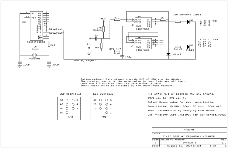
Alternative display methods exist beyond the original 8 LED frequency counter, potentially offering improved readability and a more suitable format for QRP equipment. This document presents examples of binary decimal displays. Typically, the counter omits the MHz position, focusing...
For example, I do not understand the process of demodulation or the modulation itself, and so on. Is there someone who can understand this circuit? Could you please assist me? The circuit in question likely involves a modulation and demodulation...
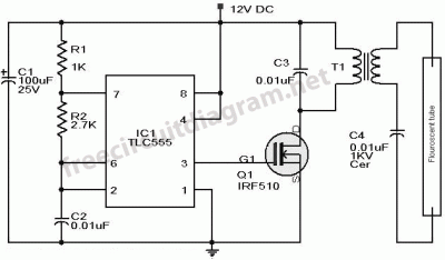
This article presents a driver circuit for a 12V, 5W fluorescent lamp. The circuit utilizes a standard 220V to 10V step-down transformer operated in reverse to achieve a 12V output. The driver circuit for a 12V, 5W fluorescent lamp is...
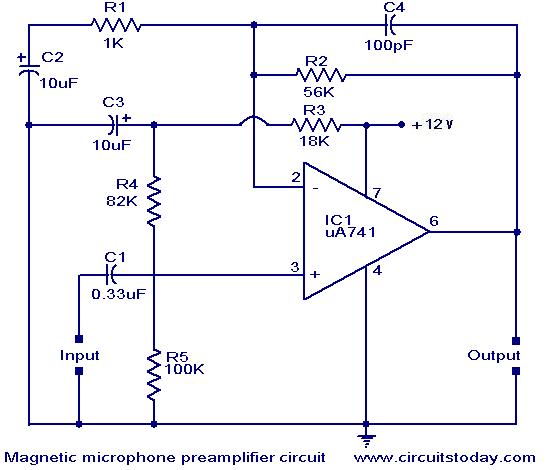
A preamplifier for magnetic pickups of record players is presented. The uA 741 is utilized as an AC-coupled non-inverting amplifier operating on a single supply. The amplifier gain is determined by the feedback components, where C2 manages the low-frequency...
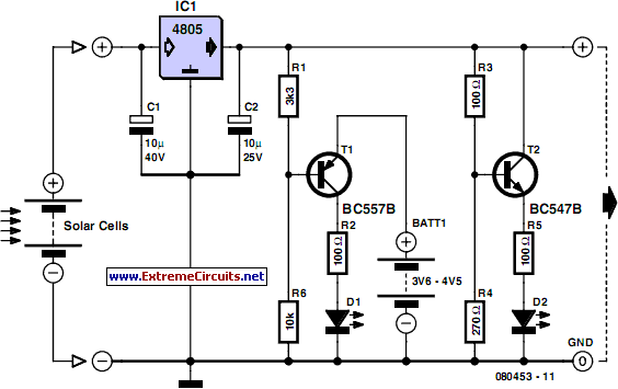
This device is designed to be a simple, inexpensive comparator intended for use in a solar cell power supply setup where a quick indication of "too low" or "just right" voltage is needed. The circuit consists of one 5V...
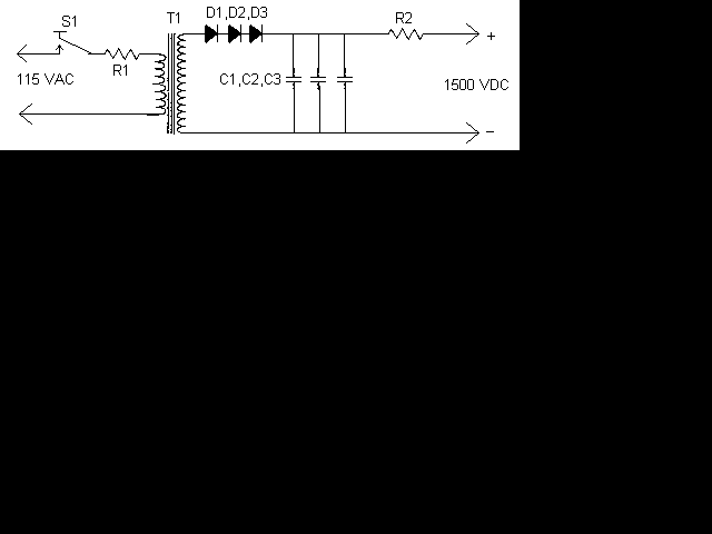
Working with lasers can be enjoyable and intriguing, but it can also be costly. High voltage power supplies for laser tubes are often more expensive than the tubes themselves. However, this power supply can be constructed using common components...