
Single Supply RS232 Interface for Bipolar AD converters

The LT1180 RS232 transceiver is a versatile component designed to facilitate communication in environments requiring robust signal integrity. It integrates a charge pump that generates low ripple voltages, thereby ensuring stable operation of connected devices such as CMOS analog-to-digital converters (ADCs) and precision voltage references. The architecture of this circuit allows it to function effectively with a single 5V power supply while maintaining a low quiescent current of just 37mA. This characteristic is particularly beneficial for battery-operated devices or low-power applications.
The LTC1094 serial ADC is sensitive to power supply noise, necessitating a clean and stable reference voltage for optimal performance. The LT1021 precision reference, utilized in this circuit, provides a low-noise 5V output derived from the LT1180’s V+ supply, ensuring that the ADC operates within its required specifications. The design effectively mitigates noise and ripple, which are critical to maintaining the accuracy of the ADC readings.
To generate the chip select (CS) signal for the LTC1094, a peak detector circuit is implemented using a single PNP transistor. This configuration ensures that the CS signal remains low for a duration that is at least equivalent to one clock period, providing sufficient time for the ADC to process the input signal. The selection of resistor (R) and capacitor (C) values is guided by the logic threshold of the LTC1094, which is approximately 1.4V. It is recommended to design the RC time constant to be at least four times the clock period while keeping the capacitance as low as feasible to enable rapid converter startup.
The design acknowledges that minor fluctuations in the CS signal do not significantly affect operation due to the level-sensitive nature of the CS pin. The PNP transistor is powered by the stable reference supply, which minimizes noise coupling into the ADC, further enhancing measurement accuracy. The peak detector's output directly drives the CMOS input of the LTC1094, making additional buffering unnecessary and simplifying the overall circuit design while maintaining reliability and performance.The LT®1180 RS232 transceiver includes a charge pump which produces low ripple supplies with suffi - cient surplus current to drive a CMOS A to D converter and precision voltage reference. The circuit in Figure 1 operates from a single 5V supply, and draws a total quiescent current of only 37mA.
These features make the circuit ideal for applications which must process bipolar signals with minimal support electronics. The LTC1094 serial A to D converter requires both a low noise supply and reference voltage for accurate operation.1 These design problems are solved with an LT1021 precision reference, which delivers a stable, low noise, 5V signal from the LT1180’s V+ output.
. The chip select signal, CS, is generated from the incoming clock with a peak detector, constructed with a single PNP transistor. R and C are designed to hold the CS pin low for at least one clock period. Assuming the logic threshold in the LTC1094 is 1.4V, two useful rules of thumb for selecting R and C are: Design RC to be at least four times the clock period.
And select C as small as possible to start the converter quickly. Minor aberrations in the CS signal are unimportant because the CS pin is level sensitive. The PNP is biased from the clean reference supply so very little noise is coupled into the A to D. Additional buffers are unnecessary because the peak detector drives a CMOS input.
Related Circuits
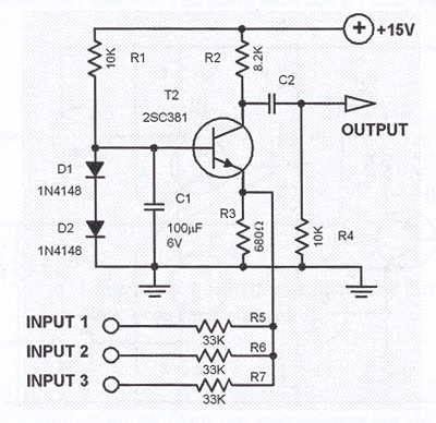
This single transistor audio mixer is utilized in an amplifier circuit design featuring a base-driven transistor, with its emitter being current-controlled. This audio mixer circuit employs a single transistor to facilitate the mixing of audio signals. The transistor operates in...
CMOS interface circuit with PMOS cross-coupled PMOS integrated circuit featuring high input impedance, where the input current can be ignored. The CMOS and PMOS interface circuit is illustrated in the accompanying figure. The CMOS interface circuit utilizing PMOS cross-coupled configurations...
Designers who build equipment for the industrial market share a widespread problem. At one extreme, they must build equipment that supports ±10V bipolar voltages, often riding on a high common-mode level, a requirement enforced by 30 years of legacy...
This schematic diagram illustrates a single-chip Theremin circuit. A Theremin is an electronic musical instrument that detects hand movements to control tones and frequency. The circuit employs two separate Colpitts LC oscillators to generate a beat frequency. The frequencies...
This circuit is a compact +5V power supply that is beneficial for digital electronics experimentation. Inexpensive wall transformers with variable output voltage can be found at electronics shops and supermarkets. While these transformers are readily available, their voltage regulation...
A simple electronic multimeter offers an affordable alternative for hobbyists deterred by the high cost of conventional multimeters. This device is designed to measure three ranges: (i) 0-15V, (ii) 0-15mA, and (iii) 0-150mA, with the possibility of extending the...