
Symmetry Feedback Maximizes Function Generators Linear Sweep Range

The internal current-source circuitry presents two challenges when the control voltage at pin 8 approaches the positive supply voltage (V+). First, due to VBE mismatch between the internal npn/pnp transistors, the voltage across R2 and R3 is at least 100 mV, which restricts the lowest effective control voltage. Second, this VBE mismatch induces a slight voltage difference across R2 and R3, leading to a significant variation in current source outputs at low control voltages, resulting in duty-cycle fluctuations and output waveform distortion. To mitigate these issues, two control loops were integrated into the circuit. IC1 operates as a voltage follower, ensuring that pin 5 of IC2 is maintained at the control voltage, thereby eliminating the internal VBE mismatch. The second symmetry feedback loop, centered around IC3, integrates the inverted square-wave output from pin 9 of IC2 and provides this integrated voltage as an additional control signal to pin 4. This configuration modifies the current through R3, thereby sustaining the square-wave duty cycle close to 50%, compensating for the inherent VBE mismatch and voltage differences across R2 and R3. Transistor Q1 serves to invert the square-wave output, ensuring that the overall negative feedback characteristic of the symmetry feedback loop is preserved. Diode D1 partially compensates for the VCE saturation voltage of Q1, allowing for an equal voltage swing at the input to the integrator. Additionally, variable resistor VR1 is utilized for initial sine wave distortion adjustment. Experimental results demonstrate the enhancements achieved through the inclusion of the voltage follower and symmetry feedback loops, as depicted in the accompanying figures.This basic VCO/waveform generator IC circuit includes a voltage follower loop (formed with IC1) and symmetry feedback loop (IC3) to eliminate an asymmetric duty cycle, which would cause distortion at low frequencies. Fig 2. The VCO used in this circuit incorporates two npn/pnp transistor pairs that buffer the control voltage entering at pin
8 so this voltage appears across R2 and R3 (connected to pins 5 and 4, respectively) with little change. Fig 3. Experimental results show that the VCO circuit using the symmetry feedback loop experienced low distortion over a sweep of more than 1000:1, even at low frequencies.
This design describes a symmetry feedback loop that maximizes the linear sweep range of a voltage-controlled oscillator (VCO). The circuit uses an ICL8038 precision waveform generator/VCO, 1 but the design could be applied to other VCOs.
The ICL8038 is a popular function generator that provides sine, square, and triangular waveforms simultaneously over a wide frequency range ”1000:1. However, this range has been impossible to achieve without an asymmetric duty cycle and, therefore, higher distortion at lower frequencies.
2 The symmetry feedback loop maintains the duty cycle close to 50% over a frequency sweep of greater than 1000:1, providing a sine wave with low distortion. IC2, the ICL8038, forms the core of the circuit ( Fig. 1 ). The control voltage, fed into pin 8, is buffered by two independent internal npn/pnp transistor combinations and appears at pins 4 and 5 with little change ( Fig.
2 ). The voltages across R2 and R3 control two current sources in such a way that capacitor C1 is charged continuously by the current through R2 and discharged, through a switch, by twice the current through R3, based on an internal flip-flop switched alternately when the voltage across C1 reaches one-third and two-thirds of the supply voltage. The flip-flop signal is provided as an open-collector, square-wave output at pin 9. If R2 and R3 are equal, the linear charge and discharge of C1 by the equal currents produces a symmetric triangular waveform.
Pin 3 is the buffered triangle waveform across C1, and pin 2 is the sinusoidal output of an internal triangle-to-sine shaping network. The internal current-source circuitry creates two problems when the control voltage at pin 8 approaches V+.
First, because of the VBE mismatch between the internal npn/pnp transistors, the voltage across R2 and R3 is a minimum of 100 mV or more, limiting the lowest effective control voltage. Second, this VBE mismatch also causes a slight difference between the voltages across R2 and R3, which leads to a significant difference in current source currents at low control voltages.
The difference manifests as duty-cycle variation and distortion of the output waveform. Two control loops were added to the circuit in Figure 1 to reduce this variation and distortion. IC1 forms a simple voltage follower to maintain IC2`s pin 5 exactly at the control voltage, eliminating the internal VBE mismatch. The second symmetry feedback loop is built around IC3. This loop integrates the inverted square-wave output at IC2`s pin 9 and feeds the integrated voltage as an additional control-voltage signal to pin 4.
In operation, the current through R3 is modified in such a way that the square-wave duty cycle is maintained close to 50%, overriding the inherent VBE mismatch and slight difference between the voltages across R2 and R3. Transistor Q1 inverts the square-wave output so the overall negative-feedback sense of the symmetry feedback loop is maintained, and diode D1 compensates partially for the VCE saturation voltage of Q1 so the input to the integrator has an equal voltage swing.
VR1 is used for initial distortion adjustment of the sine wave. Figure 3 shows measured results that illustrate the improvements over the basic circuit by the addition of the voltage follower and symmetry feedback loops. T 🔗 External reference
Related Circuits
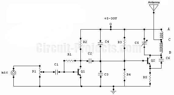
This is a well-designed basic FM transmitter that allows the reception of transmitted signals within a range of 1-2 km using a standard FM receiver. Additionally, the circuit features a coil mounted on the printed circuit board. The amplitude...
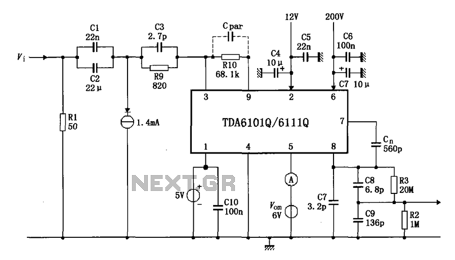
The test circuit features a feedback factor of 1/83 utilizing the DA6101Q/6111Q. The input signal is fed through a network comprising resistors R1 and R9, and capacitors C1, C2, and C3, entering the TDA6101Q, which includes three pins for...
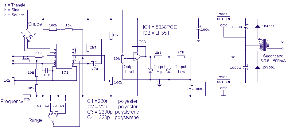
Built around a single 8038 waveform generator IC, this circuit produces sine, square or triangle waves from 20Hz to 200kHz in four switched ranges. There are both high and low level outputs which may be adjusted with the level...
The transmitter circuit described here includes an additional RF power amplifier stage following the oscillator stage, which increases the power output to 200-250 milliwatts. When used with a properly matched 50-ohm ground plane antenna or a multi-element Yagi antenna,...
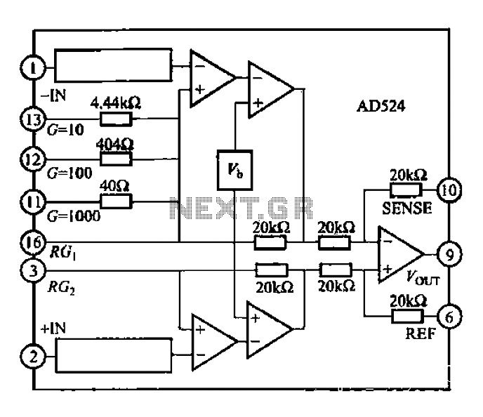
The AD524 is a low-drift instrumentation amplifier characterized by a drift voltage of 0.5 mV and a maximum drift of 25 mV at room temperature. It has low noise performance with a noise level of 0.3 mVp-p in the...
The FM transmitter circuit operates within the broadcast band of 88 to 108 MHz and can be utilized to transmit audio signals for remote listening. The output power... The FM transmitter circuit is designed to function within the frequency range...