
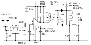
Test circuit diagram with feedback factor of 1 83 of TDA6120Q
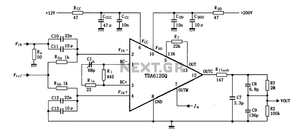
The TDA6120Q is a versatile integrated circuit designed for use in various audio and video applications. It features a differential input stage that effectively amplifies the input signal while maintaining low noise levels. The configuration of resistors and capacitors in the circuit plays a crucial role in shaping the signal and ensuring stability.
The input stage, consisting of Ra, C10, and C11, serves to filter and condition the incoming signal before it reaches the differential inputs. This is critical for achieving high fidelity in the output. The differential inputs at pins 2 and 3 allow for common-mode noise rejection, enhancing the overall signal integrity.
The amplified output from pin 12 is further processed through a network of resistors and capacitors, which serve to adjust the frequency response and gain of the circuit. The feedback resistor (Rf) connected to pin 13 is integral to maintaining stability and controlling the gain of the amplifier, allowing for dynamic range expansion in the output signal.
The pre-emphasis network, formed by Ri, Rin, and C1, is essential for compensating for signal losses at higher frequencies, ensuring that the output maintains clarity and detail. This network is particularly important in applications where signal degradation may occur due to transmission over long distances.
The inclusion of Rflash at the output provides critical protection against voltage spikes, which can occur during sudden changes in load or external disturbances. This resistor limits the current and protects the circuit from potential damage, thereby enhancing the reliability of the system.
For proper operation, it is essential to include decoupling capacitors at Vcc and VDD. The use of both ceramic and electrolytic capacitors in parallel ensures that the circuit is adequately decoupled across a wide frequency range, minimizing the risk of oscillations and ensuring stable operation under varying load conditions. This design consideration is vital for maintaining the performance of the TDA6120Q in real-world applications.Feedback has shown TDA6120Q factor 1/83 test circuit shown in Figure. Input signal Vi composed by Ra, C10, C11 input into the network TDA6120Q 2 feet, 2 feet and 4 feet are ins ide the differential input stage inverting input terminal and non-inverting input, the amplified signal from 12 feet out, after by the Rflash, R2, R3, C7, C8, C9 network of output. Resistance between 13,5 feet Rf is the feedback network, the output from the expansion of the dynamic range of action.
Resistance between 1,3 feet Ri, Rin and capacitor C1 constitute a pre-emphasis network. The output end of the resistor Rflash cathode discharge protection, when a high voltage discharge, serves to limit the current and voltage limiting effect. Vcc (6 feet), VDD (10 feet) must be added decoupling capacitors, high-frequency decoupling capacitance characteristics of a good ceramic capacitors and electrolytic capacitors connected in parallel.
Related Circuits
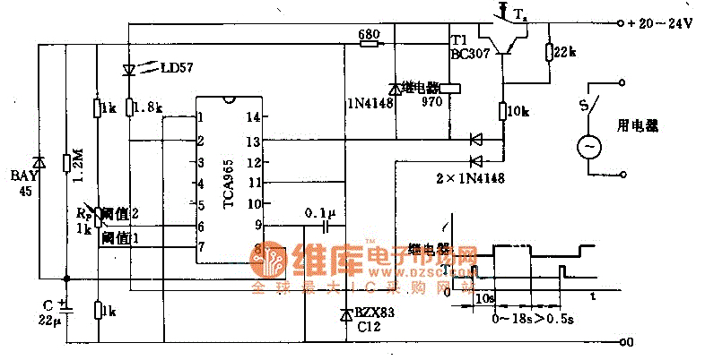
The foot 13 between valve value 1 and valve value 2 will draw the transistor base current. If the relay releases, after a recovery time of 0.5 seconds, pressing the key will initiate the switching process again. The timer...

The circuit of the easy-to-use LM3sDZ temperature detection system does not provide an adjusted output to obtain a 1 (hnV/°C) temperature change range if the temperature is between 0°C and a specified limit. The output voltage ranges from 0...
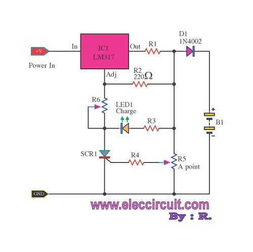
When building a lead-acid battery charger for a 6V or 12V battery, there are various methods available. One preferred option is the use of the IC LM317. The LM317 is a versatile adjustable voltage regulator that can be effectively utilized...
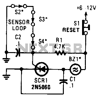
A string of three series-connected, normally closed switches is connected across the gate of a silicon-controlled rectifier (SCR). When one switch opens, the SCR is triggered through resistor R1, activating an alarm. The alarm is designed to be of...
The LM380 is a power audio amplifier designed for consumer applications. To minimize system costs, the gain is internally fixed at 34 dB. It features a unique input stage that allows for ground-referenced input signals. The output automatically self-centers...
This is a convenient design for a transistor tester. The advantage of this circuit is that transistors can be tested without actually doing the circuit soldering. The tester uses two ICs: an NE 555 timer and a CMOS IC...