
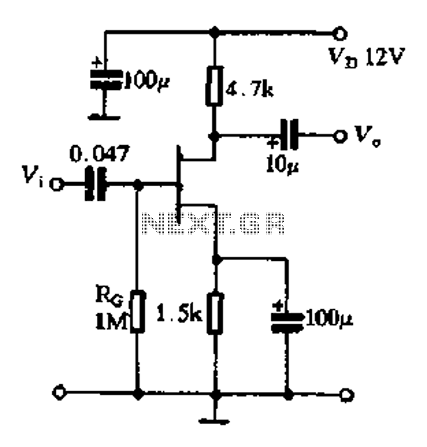
The basic FET amplifier circuit a
FETs (Field Effect Transistors) are critical components in modern electronic circuits due to their unique electrical characteristics. The high input impedance of FETs allows them to minimize signal loading on preceding stages, making them ideal for applications where signal integrity is paramount. The low noise figure of FETs further enhances their suitability for sensitive applications, such as RF amplification and audio processing.
The common source configuration is one of the most widely used FET amplifier topologies. In this configuration, the input signal is applied to the gate terminal, and the output is taken from the drain terminal. This setup provides voltage gain and is often employed in signal amplification applications. The common gate configuration, while less common, is beneficial for applications requiring low input capacitance and high-frequency response, as it presents a lower impedance to the source signal. The common drain configuration, also known as a source follower, is used primarily for impedance matching, providing a unity gain while offering a high input impedance.
When designing circuits with FETs, the impact of parasitic capacitances must be taken into account. The Miller effect can significantly affect the frequency response of FET amplifiers, particularly in high-frequency applications. Designers often implement techniques such as negative feedback or additional compensation networks to mitigate these effects and improve stability.
In low-frequency applications, the high input impedance of FETs can make circuits susceptible to noise pickup. Therefore, effective shielding and grounding techniques are essential to minimize interference from external sources. Proper layout design and the use of twisted pair wiring can further enhance the performance of FET-based circuits.
In summary, FET amplifiers offer a versatile solution for various electronic applications, with configurations that cater to specific needs. Understanding their characteristics and the associated design considerations enables engineers to effectively utilize FETs in both low and high-frequency circuit designs.FET having a high input impedance, the noise figure is small, anti-crosstalk, good mutual interference term performance, etc., in the electronic circuits used more and more wid ely. FET amplifier transistor amplifiers to be like that, configured as a common source (equivalent to a total emission) amplifier, a common-gate (equivalent common base) amplifier and a common drain (equivalent to common collector) amplifier. And it can also form a common source common source amplifier, total gate amplifier common source and common drain amplifier source altogether complex circuit form, as 8-50 and crystal corresponding transistor amplifier FET amplifier also has the characteristics of the corresponding 6 is similar to the transistor circuit to be noted that in FET amplifier, since the high input resistance of FET gate, the front and rear stage circuit when the cascade circuit, basically without considering the impact on the post-stage circuit of the preceding stage, thereby simplifying the design and debugging.
However, because of its high input impedance A, distributed capacitance, inter-electrode capacitance and the Miller effect capacitance affect more than the transistor circuits are critical, therefore, still in use in high-frequency circuits and gate circuits and total common source circuit, a total common source-drain circuit peers formula to improve the stability and frequency characteristics of the amplifier. In the low-frequency amplifier circuit, due to the high input impedance FET, easily induced hum and other noise signal, because this process should pay more attention to shielding and other issues.
Related Circuits
One of the advantages of hosting a hobby website is the opportunity to connect with individuals via email who share similar interests. Since posting Bruce's initial OddWatt project on the site, communication has occurred with numerous DIY hobbyists who...
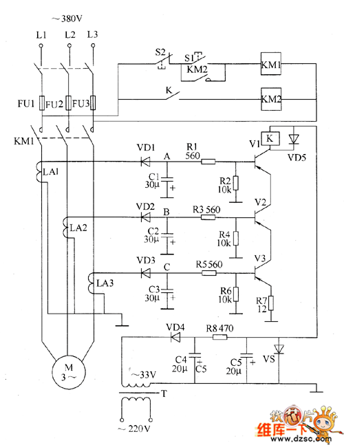
The motor protection circuit consists of a power supply circuit, a current detection circuit, and a protection control circuit, as depicted in the accompanying diagram. The power circuit includes a power transformer (T), a rectifier diode (VD4), filter capacitors...
This metal detector circuit needs to be powered using a 9 volts power supply (DC) or a 9 volts battery. The C1 capacitor is a variable capacitor with a value of 365 pF, C2 is a 100 pF silver...
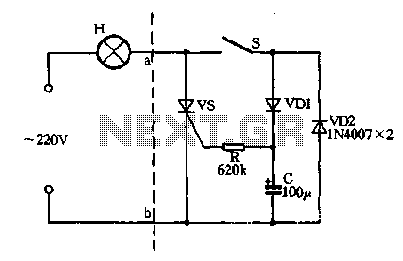
Closing the switch S allows the AC positive half-cycle to flow through diode VDI and resistor R, causing the SCR to open simultaneously at both ends of the capacitor C, which becomes fully charged. During this phase, the positive...
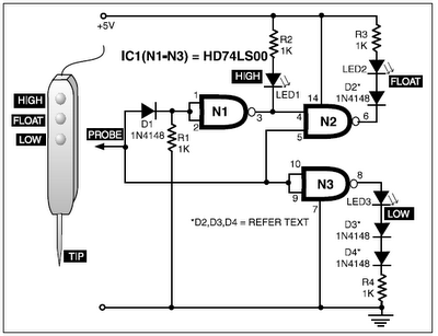
The circuit presented utilizes NAND logic gates from the Hitachi HD series, specifically the HD74LS00, which is a quad NAND integrated circuit. A special technique has been implemented to achieve three-state operation using a single IC. Gate N1 is...

A wideband high-frequency amplifier circuit is presented, utilizing resistance and capacitance coupling in a common emitter configuration to amplify high-frequency signals. When a high-frequency signal with an input impedance of 50 ohms is applied to the amplifier through a...
Warning: include(partials/cookie-banner.php): Failed to open stream: Permission denied in /var/www/html/nextgr/view-circuit.php on line 713
Warning: include(): Failed opening 'partials/cookie-banner.php' for inclusion (include_path='.:/usr/share/php') in /var/www/html/nextgr/view-circuit.php on line 713