
Timer circuit

The circuit described functions as an adjustable timer utilizing a 555 timer IC (IC1) configured in astable mode to generate clock pulses. When power is applied, IC1 begins to oscillate, producing a continuous square wave output. This output is fed into the clock input of the 4017 decade counter (IC2), which counts the pulses from the 555 timer. The 4017 outputs a high signal on its respective output pins in response to the clock pulses, effectively counting up to 10 before resetting.
In this design, the output from the 4017 is connected to the 4020 binary counter (IC3), which further counts the pulses generated by the 555 timer. The 4020 is capable of counting up to 8192 (2^13), which is determined by the configuration of its internal flip-flops. Once the combined count of the two ICs reaches the preset value, the output from the 4020 goes high.
The transistor Q1 (BC214) serves as a switch that is activated by the output of the 4020. When the output of IC3 transitions high, it turns on Q1, which can then control a load, such as a relay (RL1). The relay is used to switch on or off a connected device, allowing for the timer functionality. The relay in this circuit is rated for 12V and requires a minimum of 120 ohms for proper operation.
The timing interval can be adjusted using the potentiometer RV1, which varies the resistance in the timing circuit of the 555 timer. The overall range of the timer can be set between 1 minute and 20 hours by selecting appropriate resistor and capacitor values in conjunction with the 555 timer's configuration.
The component list includes:
- R1 = 2.2kΩ
- R2 = 39kΩ
- R3 = 1MΩ
- R4 = 27kΩ
- R5 = 12kΩ
- R6 = 6.8kΩ
- C1 = 120nF 63V polyester
- C2 = 1.2μF 63V polyester
- C3 = 100nF 63V
- RV1 = 470kΩ potentiometer
- S1 = 2x3 selection switch
- S2 = Push button (normally open)
- D1-2 = 1N4001 diode
- IC1 = LM555 timer
- IC2 = 4017B decade counter
- IC3 = 4020B binary counter
- Q1 = BC214 transistor
- RL1 = 12V relay (>120Ω)
This circuit design provides a versatile and adjustable timer solution suitable for various applications requiring delayed operation.A wide rage auto turn OFF timer covering 1 minute to 20 hours in three ranges with S1. As soon as power is applied to the circuit the IC1 [555] starts to oscillate happily and feeds clock pulses to the IC2 [4017]. The IC2 [4017] and IC3 [4020] give a combined count rate of 81920 before the output of the IC3 [4020] goes high and turns Q1 on.
With pot RV1 adjust the Time. Part List R1=2.2Kohm C1=120nF 63V polyester IC2=4017B R2=39Kohm C2=1.2uF 63V polyester IC3=4020B R3=1Mohm C3=100nF 63V Q1=BC214 R4=27Kohm RV1=470Kohm pot. S1=2X3 SEL SWITCH R5=12Kohm D1-2=1N4001 S2=Push button no R6=6.8Kohm IC1=LM555 RL1=12V >120ohm Relay
🔗 External reference
Related Circuits
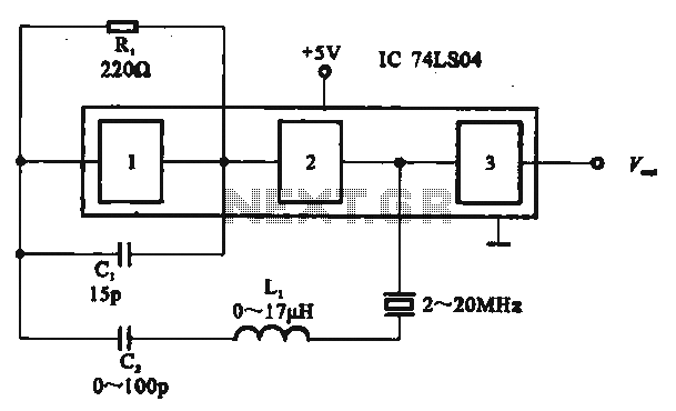
The circuit includes several gates arranged as a crystal oscillator circuit. Figure (A) illustrates a crystal oscillator circuit operating at 1 MHz, while Figure (B) depicts a 20 MHz crystal oscillator circuit. Figure (C) represents a variable crystal oscillator...
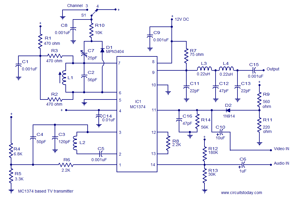
A simple TV transmitter circuit utilizing the TV modulator circuit IC MC1374. It operates with a 12V supply and is capable of broadcasting on channel 3 or 4, employing FM modulation for sound transmission. The TV transmitter circuit based on...
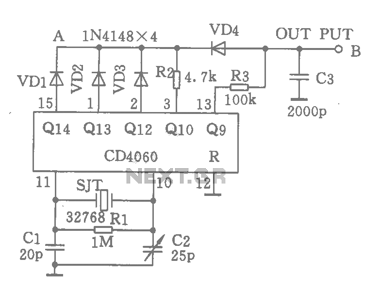
A CD4060 integrated circuit, combined with a 32,768 Hz crystal oscillator, is utilized to create a highly accurate clock source that generates 60 pulses per second. The operation is based on the division of the 32,768 Hz pulse output...
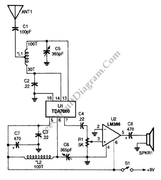
An AM radio receiver circuit utilizing an FM IC chip as the primary component. This AM radio receiver circuit incorporates hand-wound coils to adjust the frequency within the AM bandwidth. The AM radio receiver circuit is designed to capture amplitude-modulated...
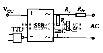
This document discusses the AC solid-state relay (AC-SSR) and presents its basic application circuit as illustrated in Figure (a). Additionally, it includes a TTL drive SSR circuit depicted in Figure (b), a CMOS driver circuit for the SSR shown...
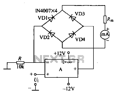
An operational amplifier, a diode bridge rectifier, and DC mA AC voltmeter tables are illustrated in the figure. The operational amplifier used is the LM324. The measured AC voltage is applied to the inverting terminal of the operational amplifier,...