
tv transmitter circuit 17
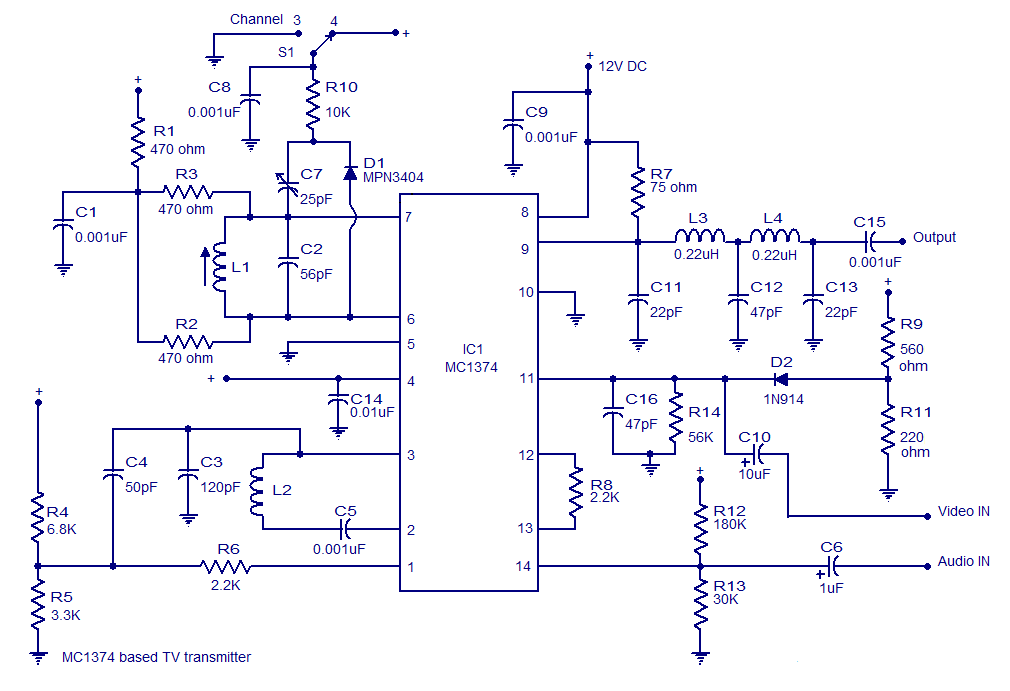
The MC1374 IC is designed to facilitate the construction of a compact and efficient TV transmitter. The integrated architecture reduces the need for numerous discrete components, thereby simplifying the design process and enhancing reliability. The inclusion of a sound carrier oscillator and an FM audio modulator allows for simultaneous transmission of video and audio signals, making it suitable for various broadcasting applications.
The Q factor, determined by resistors R1, R2, and R3, plays a crucial role in defining the bandwidth and selectivity of the RF output. A Q factor of around 15 ensures optimal performance for the intended application. The gain of the modulator can be adjusted via resistor R8, allowing for flexibility in output levels based on specific transmission requirements.
The RF oscillator frequency of approximately 105 MHz is established through the tank circuit formed by inductor L1 and capacitor C2, ensuring that the transmitter operates within the desired frequency range for television broadcasting. The double pi low-pass filter, consisting of L3, L4, C11, C12, and C13, effectively suppresses unwanted harmonics, which is critical for maintaining signal integrity and compliance with broadcasting standards.
The design also incorporates several decoupling capacitors (C6, C10, and C9) to mitigate power supply noise, ensuring stable operation of the transmitter. The biasing networks for both the video and audio inputs (R9, R11, R12, and R13) are essential for proper signal conditioning, allowing for a clean and reliable input to the modulator.
Overall, the MC1374-based TV transmitter circuit is a robust solution for low-power television broadcasting, combining ease of use with high-quality signal transmission capabilities.A very simple and high quality TV transmitter circuit based on IC MC374 is shown in this article. MC1374 is an integrated TV modulator circuit that can be used in various TV transmitter applications. The MC1374 includes all necessary circuitries required for a TV modulator such as sound carrier oscillator, FM audio modulator, dual input RF modulato
r etc. The IC packed with a lot of great features like wide dynamic range, single supply operation, low distortion, variable gain radio frequency modulator section, minimum intermodulation distortion, + or Sync etc. The IC requires few external components and can be operated from a supply voltage range from 5 to 12V DC.
The circuit diagram of the TV transmitter using MC1374 is shown below. The video signal input to the circuit can be either negative or positive. The RF output will be approximately zero when the voltages at pin 1 and 11 are equal and the RF output increases linearly as the difference in voltage increases. Resistors R1, R2 and R3 determines the Q factor of the circuit are here their values are so chosen that the Q factor is around 15 which is the desired value for this IC.
Resistor R8 connected between pins 12 and 13 sets the modulator gain. The RF output is available from pin 9 which is actually a source which drives a load connected from positive supply line to pin 9. The frequency of the RF oscillator is controlled by the tank circuit comprising of components L1 and C2 connected in association with pins 7 and 6.
With the present values of L1 and C2 the RF oscillator frequency is around 105MHz. Components L3, L4, C11, C12 and C13 forms a double pi low pass filter which filters away second harmonics from the radio frequency output. These second harmonics usually occur at very high frequencies due to small imbalances in the device. Resistors R9 and R11 forms the bias circuit for the video input pin. Switch S1 can be used for selecting channel 3 or channel 4 operations. Frequency modulation is used for transmitting the audio signals. Inductor L2 connected between pin 2 & 3 and the capacitor C3 from pin 3 to ground forms the necessary tank circuit for the FM sections oscillator.
Resistor R12 and R13 forms a biasing network for the audio input pin (pin14). C6 is the decoupling capacitor for the audio input while C10 is the decoupling capacitor for the video input. The modulate FM signal available at pin 3 of the IC is coupled pin 1 of the IC through resistor R6 and capacitor C4 and then this signal is modulated onto the AM carrier.
Capacitor C9 filters off noise if any from the power supply. R4 and R5 form a biasing network for the pin 1 of the IC. C14 a noise bypass capacitor for the oscillator B+ pin (pin14) of the IC. This pin can be used for shutting down the sound system during the alignment of the AM section. 🔗 External reference
Related Circuits

This is a simple 1-watt FM transmitter circuit that is easy to construct. It consists of four transistors, one of which serves as a stable oscillator. This is followed by a buffer stage to minimize frequency variations when adjusting...
The design of this project relies heavily on sensors, which are present in both the control module and the robot. The computer analyzes the signals from these sensors to determine appropriate output actions. The control unit utilizes potentiometers as...
The camera is oriented to look out the side of the rocket during launch and downward during descent on the parachute. An optional external mirror can be added to enable the camera to look down during lift-off. The transmitter...
Instead of concentrating on the mathematical and theoretical aspects of this simple pyro RF transmitter, the focus will be on the components within each stage. The mathematics involved in understanding how and why this circuit operates is complex and...

Below 10 MHz, the development of engineering models is relatively straightforward and not significantly influenced by printed circuit board layout. In the VHF range, parasitic circuit elements and unwanted coupling can severely impact efforts to achieve cost-effective performance without...

A low power, long-life LED flashlight circuit. Electronic Design proposed a simple circuit to resolve this in a recent article. The front end of their circuit draws less than a milliamp of extra current. The described LED flashlight circuit is...