
TYPES OF ANALOG-TO-DIGITAL CONVERTERS
Analog-to-digital converters (ADCs) serve a crucial role in converting analog signals into digital data that can be processed by digital systems. The classification into one-step and multi-step architectures reflects the different approaches to achieving this conversion.
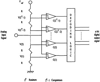
The flash ADC architecture is particularly noteworthy for its speed, as it can convert an input signal to a digital output in a single step. This is achieved through the use of multiple comparators that operate in parallel, allowing for rapid processing of the input signal. However, the requirement for a large number of comparators—specifically (2^n - 1) for an n-bit resolution—limits the practical resolution of flash ADCs. As the number of bits increases, the number of required comparators grows exponentially, leading to increased complexity and cost.
In a flash ADC, a resistive ladder is employed to create a series of reference voltages. This ladder consists of 2^n equal resistors, which effectively divides the reference voltage into 2^n discrete levels. Each level corresponds to a specific voltage that the input signal can be compared against. The output from the comparators is in the form of a thermometer code, where the number of active bits corresponds to the voltage level of the input signal.
The decoding logic is responsible for converting the thermometer code into a binary signal. This process reduces the number of bits from (2^n - 1) to n, making it suitable for digital processing. The efficiency of this conversion is crucial, as it directly affects the performance and speed of the ADC. The mapping between the thermometer code and the binary output is essential for understanding how the analog signal is represented in digital form.
In summary, the flash ADC architecture offers high-speed conversion capabilities but is limited by its resolution due to the exponential growth of required components with increased bit depth. Understanding the underlying principles of its operation, including the use of comparators, resistive ladders, and decoding logic, is fundamental for engineers designing high-performance analog-to-digital conversion systems.Analog-to-digital converters are classified into one-step architectures, such as: flash, folding and interpolative topologies, and multi-step architectures, such as: Successive approximation and pipeline topologies. The flash architecture is potentially the fastest analog-to-digital converter, because of the parallelism it employs.
However, this p arallelism puts a practical limit on the resolution of the flash analog-to-digital converter. For an n-bit analog-to-digital converter, the flash architecture employs (2 n 1) comparators and decoding logic. A resistive ladder consisting of 2 n equal resistors divides the reference voltage into 2 n equally spaced voltages as shown in Figure 7.
15 is logic 0. The decoding logic transfers the thermometer code which has (2 n 1) bits into a binary signal which has n bits. Table 7. 1 shows the mapping between the thermometer code and the binary coded signal when n=3. 🔗 External reference
Related Circuits
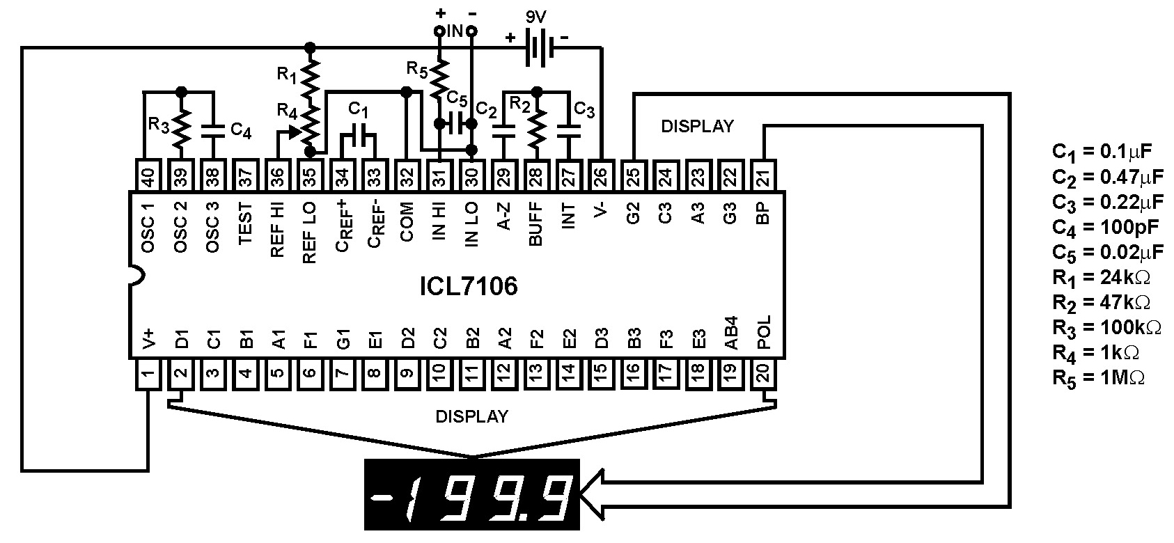
The Intersil ICL7106 and ICL7107 are high-performance, low-power, 3½ digit analog-to-digital (A/D) converters. They include seven-segment decoders, display drivers, a reference, and a clock. The ICL7106 is designed to interface with a liquid crystal display (LCD) and features a...
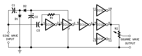
This circuit is designed to produce square waves by converting a sine wave obtained from an existing generator. A key feature is that it requires no external power source, allowing for simple connection between a sine wave generator and...
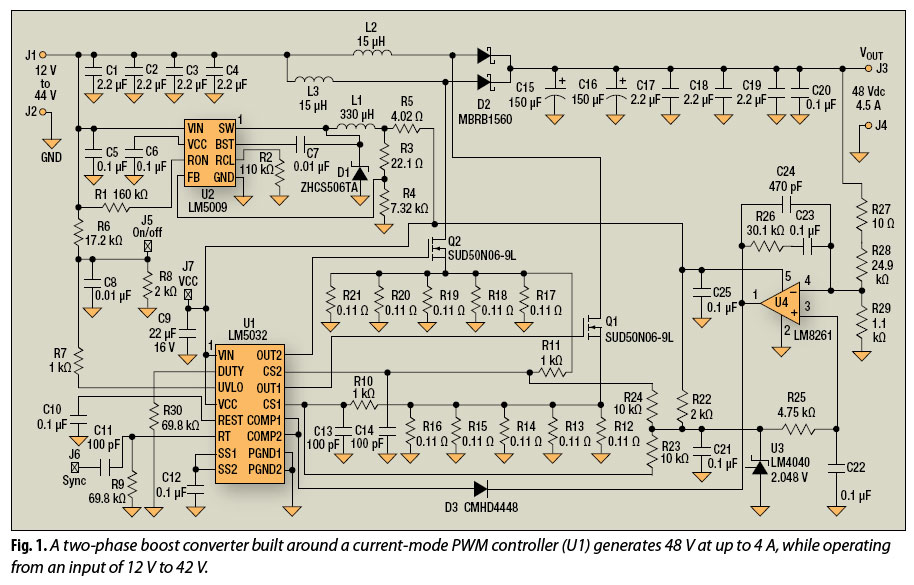
The multiphase approach has long been utilized to enhance efficiency, minimize ripple, and reduce the size of capacitors and inductors in buck converters. This method can also offer similar advantages for boost converters. The multiphase technique involves the use of...

Charger for all battery types power supply. This lithium battery charger circuit is dedicated to charging lithium batteries. It uses two chips: the voltage regulator LM317T and ICL7665, which warns microprocessors of overvoltage and undervoltage conditions. Charging is completed...
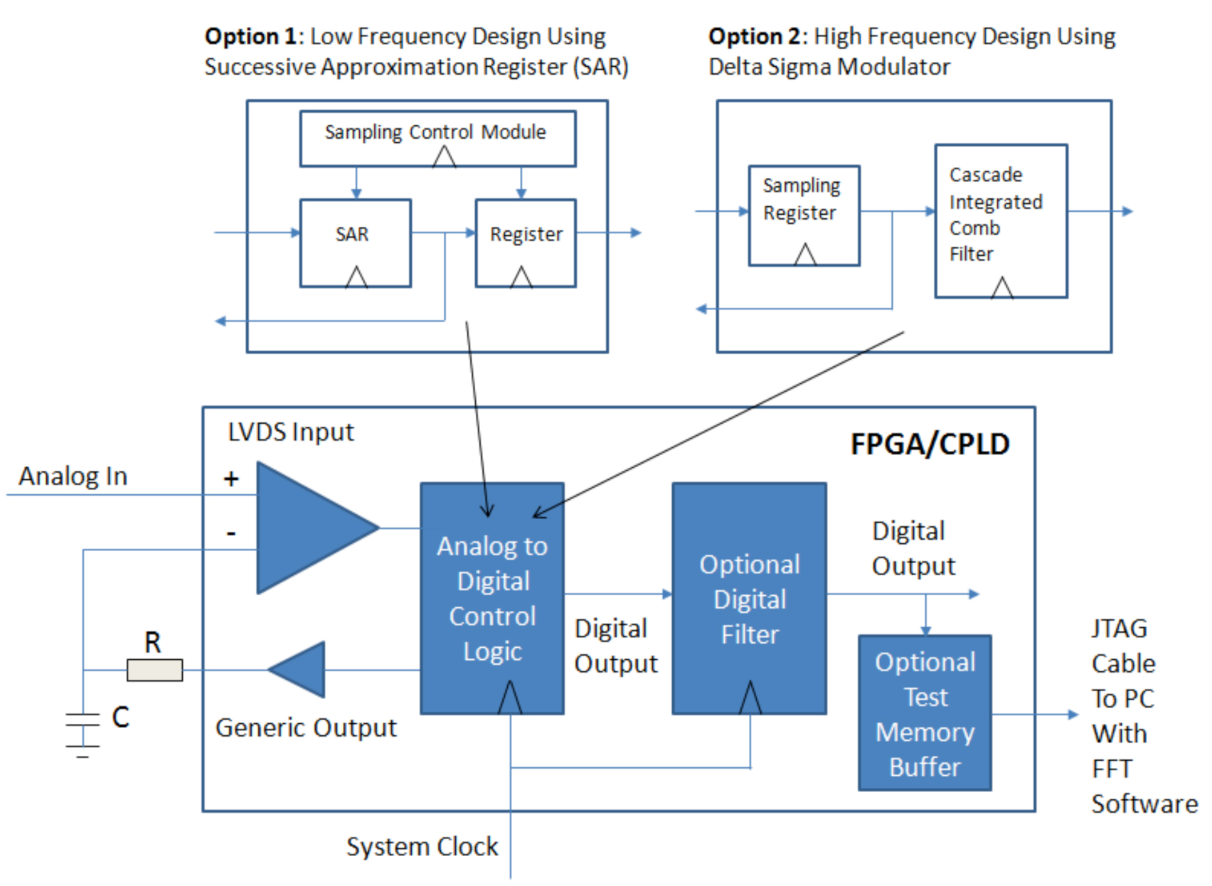
Designers of digital systems are familiar with implementing the remnants of their digital design by using FPGAs and CPLDs to connect various processors, memories, and standard function components on their printed circuit board. In addition to these digital functions,...
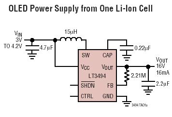
The LT3494 and LT3494A are low-noise boost converters that integrate a power switch, Schottky diode, and output disconnect circuitry. These devices utilize an innovative control technique that results in minimal output voltage ripple and high efficiency across a broad...