
USB Live Oscilloscope: ADCV Board
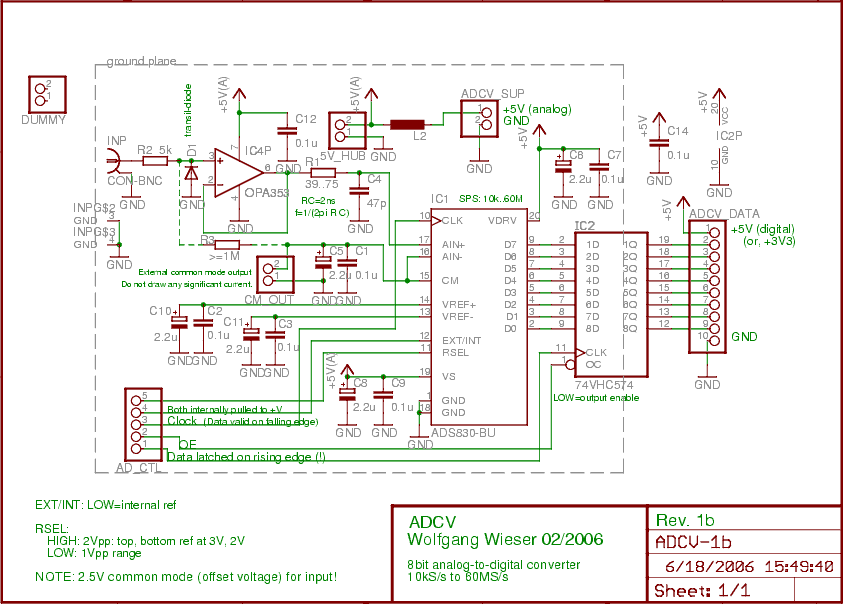
The circuit design incorporates a fast non-inverting buffer amplifier (OPA353) that serves to protect the analog-to-digital converter (ADC) from potential overvoltage conditions. By operating in a unity gain configuration, the buffer ensures that the signal integrity is maintained while preventing excessive voltage levels from reaching the ADC, thereby safeguarding its functionality.
The ADS830 ADC is selected for its cost-effectiveness and capability to handle a wide range of sampling frequencies, from 10 kS/s to 60 MS/s. Its 3-stage pipeline architecture allows for efficient processing of incoming analog signals, with the output data reflecting the sampled analog voltage from three clock cycles prior. This design choice results in a fixed delay of 300 ns when operating at a sampling rate of 10 MS/s, which is critical for timing analysis in applications where synchronization of digital and analog signals is necessary.
The AD_CTL connector plays a pivotal role in the operation of the ADC by providing both the sampling and latch clocks necessary for the conversion process. The clocks operate at the same frequency but are phase-shifted, ensuring that the ADC functions correctly during the sampling process. Additionally, the configuration options available through this connector allow for flexibility in the system design, enabling adjustments in sensitivity and reference voltage selection to accommodate various signal conditions.
The requirement for a common mode offset voltage of 2.5 V is essential for the proper functioning of the circuit, particularly in systems designed for single-supply operation. This voltage level is optimal for ensuring that the analog signals are processed correctly without distortion or clipping. When connecting to the CON-BNC connector, it is imperative to maintain this offset, as failure to do so may result in inaccurate readings or signal integrity issues.
In scenarios where different signal levels are needed, the design must include additional components, such as an input amplifier and level shifter. This enhancement will likely necessitate an external power supply to accommodate the required voltage levels, ensuring compatibility with various signal sources and measurement instruments. Overall, the described circuit design effectively balances performance, cost, and flexibility, making it suitable for a range of applications in analog signal processing.The analog input is first fed into a fast non-inverting buffer amplifier (OPA353) set up for unity gain which protects the analog-to-digital converter from out-of-range voltages. The ADS830 is a fairly cheap 8-bit analog-to-digital converter which supports sampling clocks from 10kS/s to 60MS/s.
It has sort of a 3-stage pipeline meaning that the co nversion result available on the digital outputs corresponds to the analog voltage 3 clocks earlier. Since we`re sampling on a constant 10MS/s rate (remember: for lower "sampling rates", the sampling clock is still 10MHz but we select only certain samples before committing them to the USB-FX2 FIFO) this introduces a constant delay of 300ns. This is nothing to worry about most of the time but when comparing the time from digital and analog inputs, it must be remembered that the analog signal lags somewhat behind.
The AD_CTL plug not only provides the sampling and latch clocks (they have the same frequency but opposite phase) but also the config for the AD converter allowing to set the sensitivity to 1Vpp or 2Vpp or choosing between internal and external reference. (There is currently no extra plug for an external reference. ) The analog has to be attached to the CON-BNC connector. It must be understood that the input is DC coupled and demands a common mode offset voltage of 2. 5V. This is ideal for 5V single-supply amplifier circuits which operator symmetrically around 2. 5V. However, this is not what one expects when connecting to a "real" oscilloscope. If different signal levels are required, an extra input amplifier and level shifter has to be built (which will probably require an external power supply!).
🔗 External reference
Related Circuits
The servo driver is just simply two 4017 decade counters and lots of 0.1" headers. Only populate the A side headers; the B servo bank is optional and will require a few more header pieces. If you received 20...
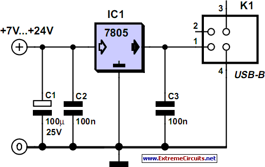
This project is designed to charge a pair of AA Nickel Metal Hydride (NiMH) or Nickel Cadmium (NiCd) cells using a laptop's USB port for power. It addresses the need for a convenient charging solution. Any USB port can...
A simple USB FM transmitter that can be used to play audio files from an MP3 player or computer on a standard VHF FM radio by connecting it to a USB port. The circuit does not require any coils...
Although a matching charger is typically included in the package, some devices can only be charged via a USB port. This is not surprising for USB MP3 players, which need to dock with a PC for file transfers. However,...
The TL082 (Or a TL072 also is OK) Creates an Adjustable Sawtooth Generator. (It also has a Square wave Output, but it isn`t used here.) The Left and Right LEDs are connected in series, and if this circuit is used...
To share a regional press like the USB printer, scanner etc. two computers, it is relatively easy. Just connect the two computers on a network device and say the printer as shared. This method however requires the continued operation...
Warning: include(partials/cookie-banner.php): Failed to open stream: Permission denied in /var/www/html/nextgr/view-circuit.php on line 713
Warning: include(): Failed opening 'partials/cookie-banner.php' for inclusion (include_path='.:/usr/share/php') in /var/www/html/nextgr/view-circuit.php on line 713