
USB Live Oscilloscope: Digital Input Board
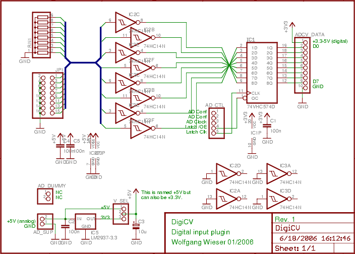
The digital input board is designed to facilitate the integration of multiple digital signals into a system, providing flexibility in terms of voltage levels and input configurations. The inclusion of pull-down resistors is critical in ensuring that the inputs remain at a defined low state when not actively driven high, thereby preventing floating inputs which can lead to erratic behavior. The choice of Schmitt-trigger devices adds noise immunity and ensures clean transitions between high and low states, which is particularly beneficial in applications where signal integrity is paramount.
The HC14 Schmitt-trigger in DIL-14 packages allows for easy replacement, which is advantageous for prototyping and testing. The option to switch to HCT14 devices for TTL compatibility provides versatility, accommodating a wider range of input signal types. This feature is particularly useful in mixed-signal applications where both CMOS and TTL logic levels may coexist.
The board's power supply considerations are noteworthy; while the LDO provides an additional 3.3V output from a 5V supply, the existing 3.3V available on the mainboard simplifies the design for systems already operating at this voltage level. It is crucial to ensure that the ADCV_DATA pin operates at the correct voltage level corresponding to the chosen input configuration to avoid potential damage or misreading of input signals. Overall, this digital input board is a robust solution for interfacing with various digital signals in electronic systems, ensuring reliability and ease of use in diverse applications.The digital input board has 8 distinct digital inputs available on JP1. There are separate pull-down resistors (RN1, choose a value you like, e. g. 1MOhm) and then each input has a Schmitt-trigger. Since these may be destroyed by improper input voltages, I chose to use HC14 devices in DIL-14 packages and mount them on sockets to be easily replaceab le. Furthermore, one can switch from CMOS to TTL levels by plugging in a HCT14 instead or even have mixed inputs since there are two Schmitt-trigger IC`s, each one handling 4 inputs. The inputs operate on 5V or 3. 3V levels; for the latter, there is an on-board LDO (IC5) which generates the 3. 3V from 5V. This is not strictly necessary since we already have 3. 3V on the mainboard (available on the AD_DUMMY connector, actually. ), so you may choose to go for a simpler design. Note that when configuring for 3. 3V inputs, the digital bus voltage at pin1 on ADCV_DATA must be 3. 3V, otherwise 5V are supported as well (although we exclusively use 3. 3V for the USB Live Oscilloscope). 🔗 External reference
Related Circuits
This is a chronological account of a project to design and build a digital clock based on the Arduino open-source architecture, utilizing the ATMEGA8 microcontroller. The ATMEGA8 is an 8-bit, 16MHz microcontroller with integrated digital and analog inputs and...
This circuit is designed for precise centigrade temperature measurement. It features a transmitter section that converts the sensor's output voltage, which is proportional to the measured temperature, into frequency. The output frequency bursts are transmitted through the mains supply...
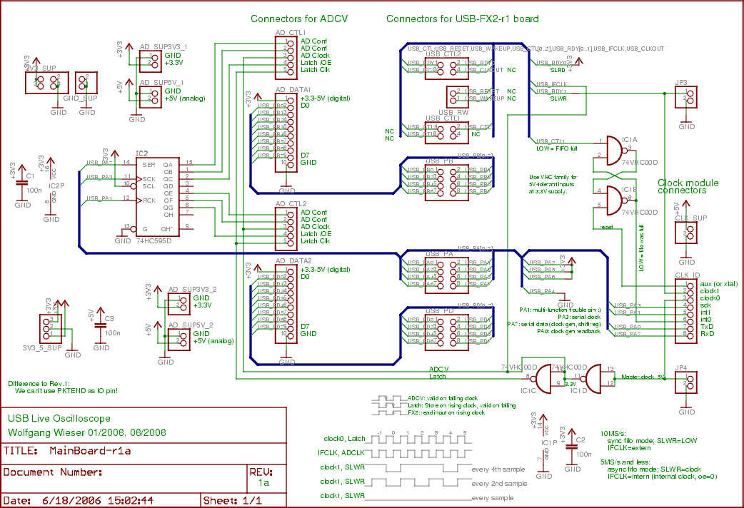
The two input boards (ADCV or digital) are connected to AD_CTL1, AD_DATA1, AD_SUP5V_1, and AD_SUP3V3_1 for the first board, with the second board using the same connections but with a suffix of 2. To transfer sampling data, the 16...
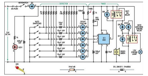
This simple alarm circuit was designed for use in a combined garage and rumpus room. It can be assembled on Veroboard and uses just one IC plus a handful of additional components. The alarm circuit is based on a single...

The circuit described is a crystal oscillation circuit using a CM OS inverting configuration, designed to ensure accurate operation. It employs a BCD counter (IC2) capable of achieving a maximum oscillation frequency of 2 MHz, which is 100 times...
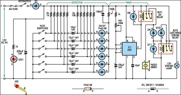
This simple alarm circuit is designed for use in a combined garage and rumpus room. It can be assembled on Veroboard and utilizes a single integrated circuit (IC) along with a few inexpensive components. The circuit is based on...
Warning: include(partials/cookie-banner.php): Failed to open stream: Permission denied in /var/www/html/nextgr/view-circuit.php on line 713
Warning: include(): Failed opening 'partials/cookie-banner.php' for inclusion (include_path='.:/usr/share/php') in /var/www/html/nextgr/view-circuit.php on line 713