
USB Live Oscilloscope: Main Board
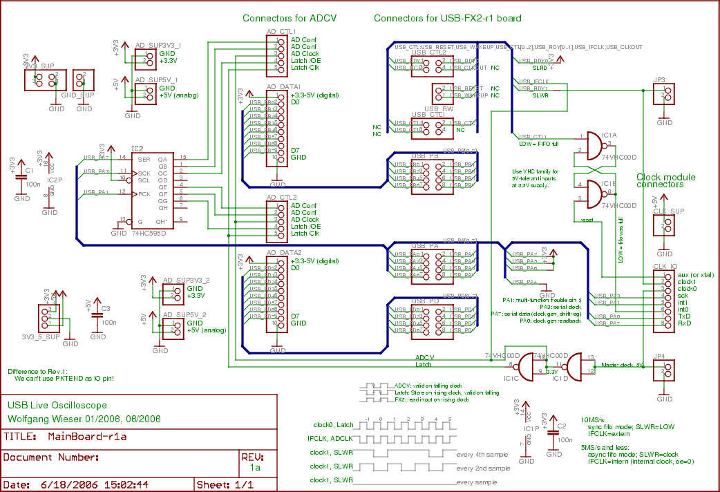
The circuit incorporates two input boards, either ADCV or digital, facilitating data acquisition through dedicated connections to the FX2-USB interface. The first board utilizes the labels AD_CTL1, AD_DATA1, AD_SUP5V_1, and AD_SUP3V3_1, while the second board mirrors these connections with a numerical suffix of 2. The architecture is designed to handle the transmission of 16 digital data lines from both input boards, which are integrated into a 16-bit wide data bus on the FX2-USB board, denoted as USB_PA.
Control signals are essential for the operation of each input board, with a maximum of three control lines available (located at pins 1, 2, and 4 of AD_CTL). These lines are managed by the 8051 microcontroller on the USB-FX2 board, utilizing specific data lines (USB_PA1, USB_PA3, and USB_PA7) along with a shift register (IC2) to facilitate control signal management.
The design includes an RS flip-flop configuration formed by IC1A and IC1B, intended to monitor FIFO buffer performance. This component plays a critical role in identifying conditions where data transfer rates are insufficient, potentially leading to buffer overflows. The flip-flop is interconnected with a clock generator, allowing it to respond to timing issues; however, it is noted that this feature is not actively utilized in the current setup. Instead, it is suggested that FIFO stalls may be effectively monitored through software interrupts implemented within the FX2 architecture.
Furthermore, the circuit addresses clock signal integrity through the inclusion of IC1C and IC1D, which are tasked with inverting the clock signals. This inversion is necessary to synchronize the ADCV clock and the interface clock with the latch clock, ensuring proper timing across the system. For a clearer understanding of the timing relationships and signal transitions, reference to the waveform diagrams provided in the schematic is recommended.The two input boards ( ADCV or digital ) get connected to AD_CTL1, AD_DATA1, AD_SUP5V_1, AD_SUP3V3_1 for the first board and the same names with suffix 2 for the second board. To transfer the sampling data, the 16 digital data lines from the two input boards are fed into the 16bit wide bus of the FX2-USB board (USB_PA, ).
Each input board can have up to 3 control lines (pins 1, 2 and 4 of AD_CTL) which are set from the USB-FX2 board`s 8051 controller via lines USB_PA1, 3, 7 and shift register IC2. IC1A, B form together an RS-flip-flop which was meant to detect FIFO buffer overflows (i. e. when the USB-FX2 board is not able to transmit data over the USB fast enough). It is connected to the clock generator so that it can take action. However, this feature currently is not used at all and the FIFO stall can probably also be detected by a software interrupt in the FX2.
IC1C, D to the necessary clock inversion because ADCV clock and interface clock need to be inverted compared to the latch clock. (See also the waveform diagrams on the schematic. ) 🔗 External reference
Related Circuits
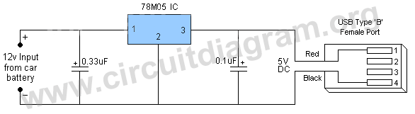
This project involves a mini USB car charger circuit that is simple to construct using only three components. The core of the circuit is the LM78M05 integrated circuit (IC), which is a 5V positive voltage regulator. This IC includes...
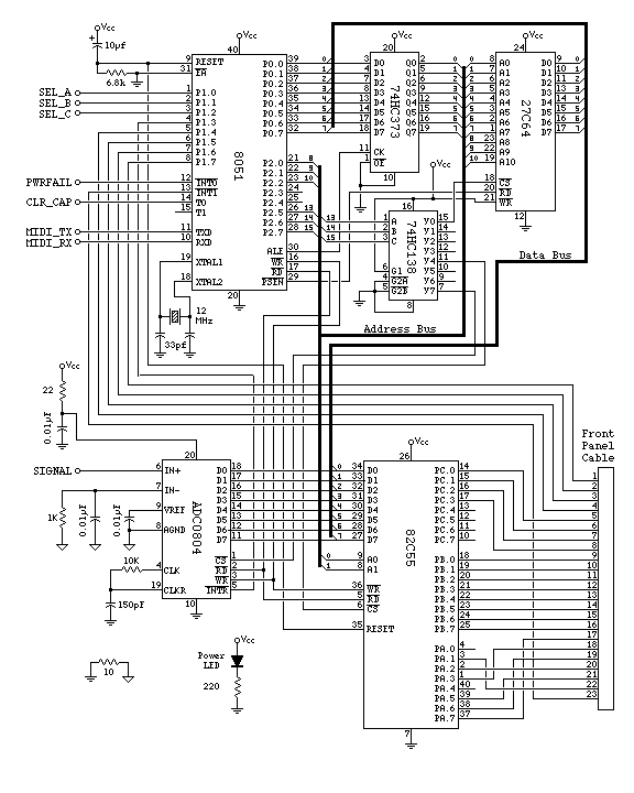
The 82C55 and seven-segment decoders on the display board will be replaced with a set of shift registers to eliminate the need for the 82C55 and the extensive wiring. The ADC0804 will be substituted with a serial interface ADC...
This demo board data sheet explains how to utilize the HV758DB1 to produce a fundamental high voltage pulse waveform for use as an ultrasound transmitting pulser. The HV758 circuit employs a DC coupling method in all level translators, eliminating...
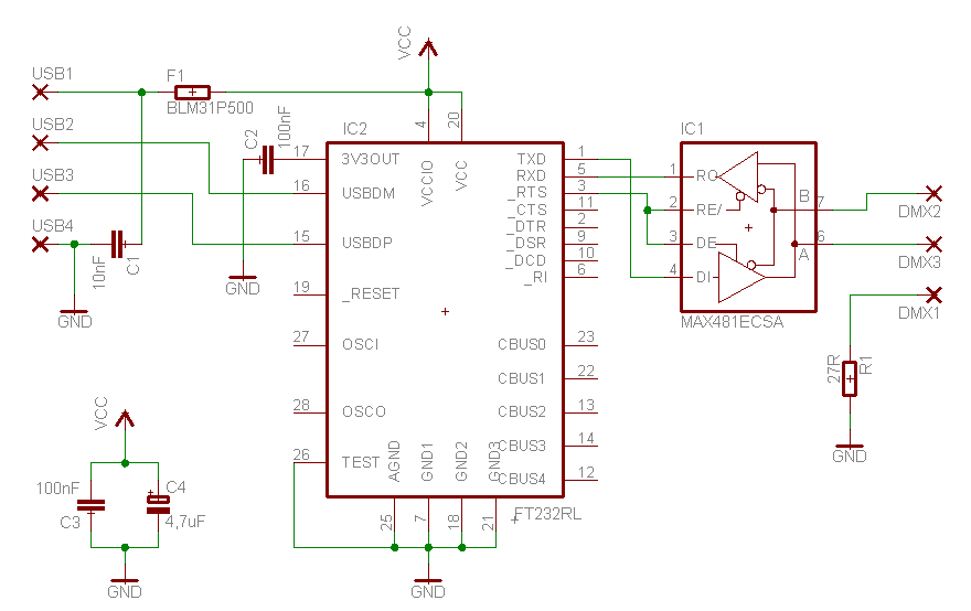
On the DMX line side, an XLR connector should be utilized, either a 3-pin or 5-pin connector. The pins in an XLR connector are typically numbered, eliminating the need for a visual reference. In the case of the 5-pin...
A board design intended for measuring a load cell has been identified with a system accuracy fault traced to the amplifier integrated circuit (IC). The output of the amplifier IC changes when the board is twisted, yielding +80mV when...

Hello everyone. This is my first post in quite some time. I obviously do not have an old enough catalog for reference. In the data section, there were references to... The input data indicates a lack of sufficient information regarding...