
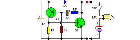
Variable corner frequency tone circuit
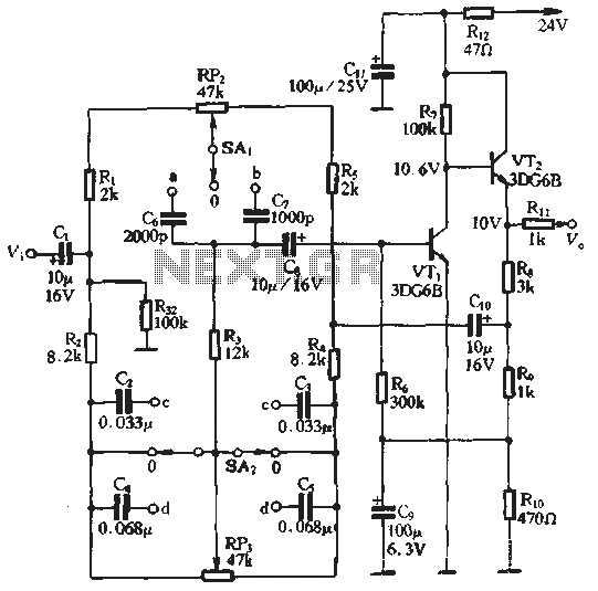
The described circuit serves as an advanced tone control system, integrating multiple components to achieve precise audio frequency adjustments. The attenuation switch plays a critical role in modifying the feedback control circuit's transition frequency, allowing for tailored audio output. The use of VTi as a common-emitter amplifier ensures that the circuit maintains a high voltage gain while preserving the phase relationship between input and output signals. The configuration of VT2 as an emitter follower enhances the circuit's input impedance, thus enabling the use of a high-value load resistor without compromising the performance of the amplifier stages.
The feedback mechanism is essential for maintaining audio fidelity and ensuring that the tone adjustments do not introduce distortion. The circuit's design incorporates resistors R and Rio to create a voltage divider that stabilizes the signal, allowing for effective feedback to the tone control circuit. This configuration enables a significant amplification of the intermediate frequency signals, enhancing the circuit's ability to manage both high and low frequencies effectively.
The selection of capacitors in conjunction with the switch positions SA1 and SA2 provides further customization of the audio output. By adjusting the capacitors, users can fine-tune the treble and bass frequencies to suit their preferences or specific audio environments. This flexibility is particularly beneficial in professional audio applications where precise sound control is paramount.
Overall, the circuit exemplifies a sophisticated approach to audio signal processing, combining feedback control, amplification, and frequency adjustment to deliver a versatile tone control solution.By selecting an attenuation switch to change the pitch of a feedback control circuit transition frequency real cases. Hu) for 2 treble controls, RP3 for bass control, SA1, SA2 are used to change the high bass control corner frequency rate. In the circuit, VTi as common-emitter amplifier, VT2 as emitter input m, the output signal with the input signal phase amplifier instead. This will not only meet the feedback tone control circuit phase requirements, and the circuit has a low output impedance.
Due to high input impedance VT2, VTi collector load resistor may be selected from a higher resistance (lOOkf7,), so that the two-stage amplifier with high voltage gain, tone control circuit which is great the balance of the circuit by dividing voltage circuit R &, and Rio will be fed back to the tone signal voltage divider circuit, so that the tone control circuit made of about three times the intermediate frequency electric voltage gain o tone control of high and low frequency from the control frequency, by SAi, Feng also choose a different capacitor to adjust. When SAi when placed d, treble control from the control frequency of 2.5kHz; when b is placed becomes 5kHzoSA2 placed c, bass controlled from the control frequency is 500Hz; when d is placed into 250 .
Related Circuits
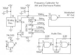
The following circuit illustrates an AM/Shortwave Radio Frequency Calibrator Circuit Diagram. This circuit is based on the 74LS93 IC. Features: The .. The AM/Shortwave Radio Frequency Calibrator Circuit utilizes the 74LS93 integrated circuit, which is a 4-bit binary counter. This...
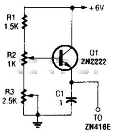
This regulator can be used with a +6-V source to supply the ZN416E low-voltage TRF radio receiver IC with the necessary +1.5 V. R3 sets the output voltage. The circuit utilizes a voltage regulator designed to convert a +6 V...
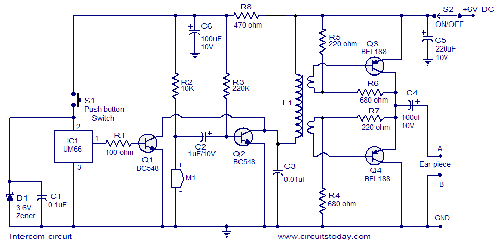
A straightforward intercom circuit designed using transistors. It does not require a changeover switch and can be used similarly to a telephone. This intercom circuit utilizes transistors to facilitate communication between two or more stations without the need for complex...
This circuit is designed to convert continuously lit lamps into flashing lights. It can be easily integrated into an existing circuit by inserting it between the lamp and the negative supply. It is particularly suitable for use with car...
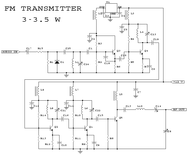
This schematic represents an FM transmitter capable of delivering an output power between 3 to 3.5 W, operating within the frequency range of 90 to 110 MHz. While the stability of the circuit is acceptable, the integration of a...

A Countdown Timer Circuit is a project submitted by a group of students for their ECE 130 - Computer Application class on August 31, 2006, at the University of St. La Salle, Philippines. The seven-segment decoder is utilized in...