
Variable-Voltage Reference Source
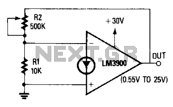
The described circuit is a non-inverting amplifier configuration using an operational amplifier. In this setup, the non-inverting input (positive terminal) is connected to ground, establishing a reference point for the inverting input (negative terminal). The gain of the circuit is controlled by the feedback resistor R2 and an additional resistor R, forming a voltage divider that determines the feedback ratio.
The gain (Av) of a non-inverting amplifier can be expressed as:
\[ Av = 1 + \frac{R2}{R} \]
When R2 is adjusted, the circuit's gain varies accordingly. Setting R2 to zero results in a gain of 1 (unity gain), which implies that the output voltage follows the input voltage closely, producing an output of 0.55 V. This is useful in applications where a buffered output is required without amplification.
On the other hand, increasing R2 to its maximum value allows the circuit to achieve a gain of 50. This configuration amplifies the input signal significantly, yielding an output voltage of approximately 25 V, which is suitable for driving loads that require higher voltage levels.
The circuit is designed to provide stable output regulation, making it effective for applications where a consistent voltage is necessary. The ability to supply several milliamps of output current indicates that this amplifier can drive small loads without significant voltage drop or distortion.
However, one limitation of this circuit is the lack of temperature compensation for the output voltage. Variations in temperature can affect the performance of the op-amp and the resistors, potentially leading to drift in the output voltage. To mitigate this issue, additional components such as temperature sensors or compensation networks may be considered in more critical applications where output stability is paramount. The noninvertiiig terminal of the op amp is grounded, and the circuit uses the voltage at the inverting t erminal as a reference. Its voltage gain is determined by the R2/R ratio. When R2 is set at zero, the circuit has unity gain and a 0.55-V output. When R2 is set to the maximum value, the circuit has a gain of 50 and an output of about 25 V. The circuit provides good regulation and can supply output currents of several milliamps. The output voltage however, is not temperature compensated. 🔗 External reference
Related Circuits
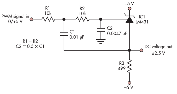
This simple circuit converts a 5V PWM signal into a variable precision reference voltage with a range of -2.5V to +2.5V. Many designs, such as a digitally controlled power supply or a programmable dummy load, require a Digital to...
This setup can function as a cost-effective current source with an output accuracy of 1%. However, the voltage offset can activate the current source even when Vqq equals Vin. Modifying the configuration of Figure 1 can resolve the issue...
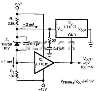
A method for enhancing the output current of a reference while also providing overload protection is illustrated. In this configuration, IC1 functions as a power buffer. The LT1027 regulates the output voltage (Vout) and ground to maintain a stable...
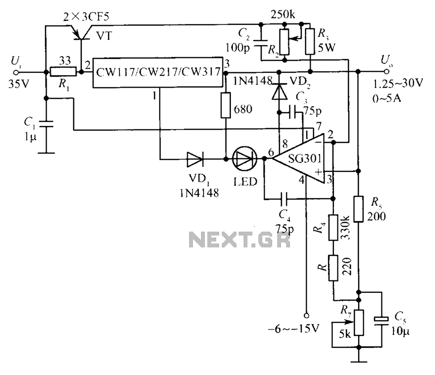
This document presents a diagram of a constant voltage/current power supply box. It is composed of three main components: spread current, constant voltage, and constant current. The design features two 3CF5 power transistors arranged in parallel, functioning as an...
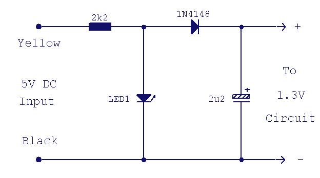
This is a replacement power source for 1.3V mercury cells or other small batteries. It has many uses and I use this circuit in my computer to power a front panel multi adapter which has a digital thermometer. The described...
The circuit is designed to provide several constant current outputs to the load resistor RL. The first RL is floating and is rarely utilized. The second RL serves as a virtual ground and is not commonly used either. The...