
Wide range oscillator
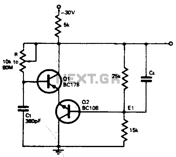
The circuit described utilizes a timing resistor R, which plays a crucial role in determining the oscillation frequency of the circuit. The adjustable range from 10 kΩ to 50 MΩ allows for fine-tuning of the timing characteristics, enabling the circuit to function effectively across a wide frequency spectrum from 400 kHz down to 100 Hz.
In this configuration, the timing resistor is connected to the collector of transistor Q1. This connection is vital as it ensures that Q1's base current is sourced exclusively from the timing capacitor Ct. The timing capacitor is responsible for charging and discharging, which in turn influences the switching behavior of the transistors in the circuit. When the transistors are in the off state, the timing capacitor charges to a voltage level that is determined by the combined base-emitter voltages of both transistors Q1 and Q2. This relationship is critical for maintaining the desired timing intervals and ensuring reliable operation of the circuit.
As the timing capacitor Ct reaches its designated voltage, it triggers the conduction of the transistors. The inclusion of capacitor Cs serves to enhance the speed of this transition, which is essential for achieving rapid switching and maintaining the integrity of the oscillation. A value of approximately 100 pF for capacitor Cs is recommended, as it provides an optimal balance between speed and stability in the timing characteristics of the circuit.
Overall, this configuration demonstrates a well-thought-out design that effectively utilizes the characteristics of resistors and capacitors to control timing and switching within the circuit, ensuring precise frequency modulation and reliable performance.Timing resistor R may be adjusted to any value between 10 K and 50 M to obtain a frequency range from 400 kHz to 100 Hz. Returning the timing resistor to the collector of Q1 ensures that Q1 draws its base current only from the timing capacitor Ct.
The timing capacitor recharges when the transistors are off, to a voltage equal to the base emitter voltage of Q2 plus the base emitter drops of Q1 and Q2 The transistors then start into conduction. Capacitor Cs is used to speed up the transition. A suitable value would be in the region of 100 pF. 🔗 External reference
Related Circuits
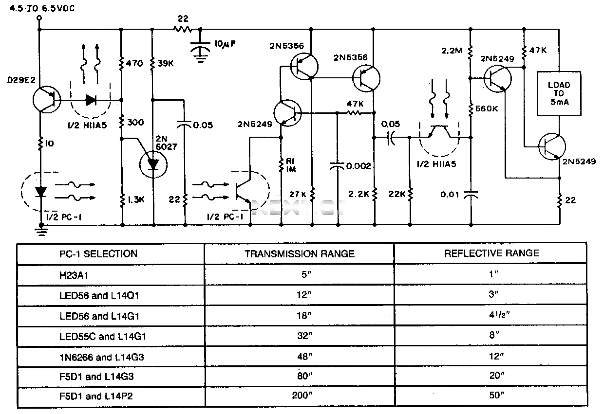
In applications requiring long-range operation with infrared (IR) light sources and high system reliability, pulsed-mode operation of the IR source is essential. Enhanced operational reliability is achieved through synchronous detection of the photodetector current, as implemented in this circuit....
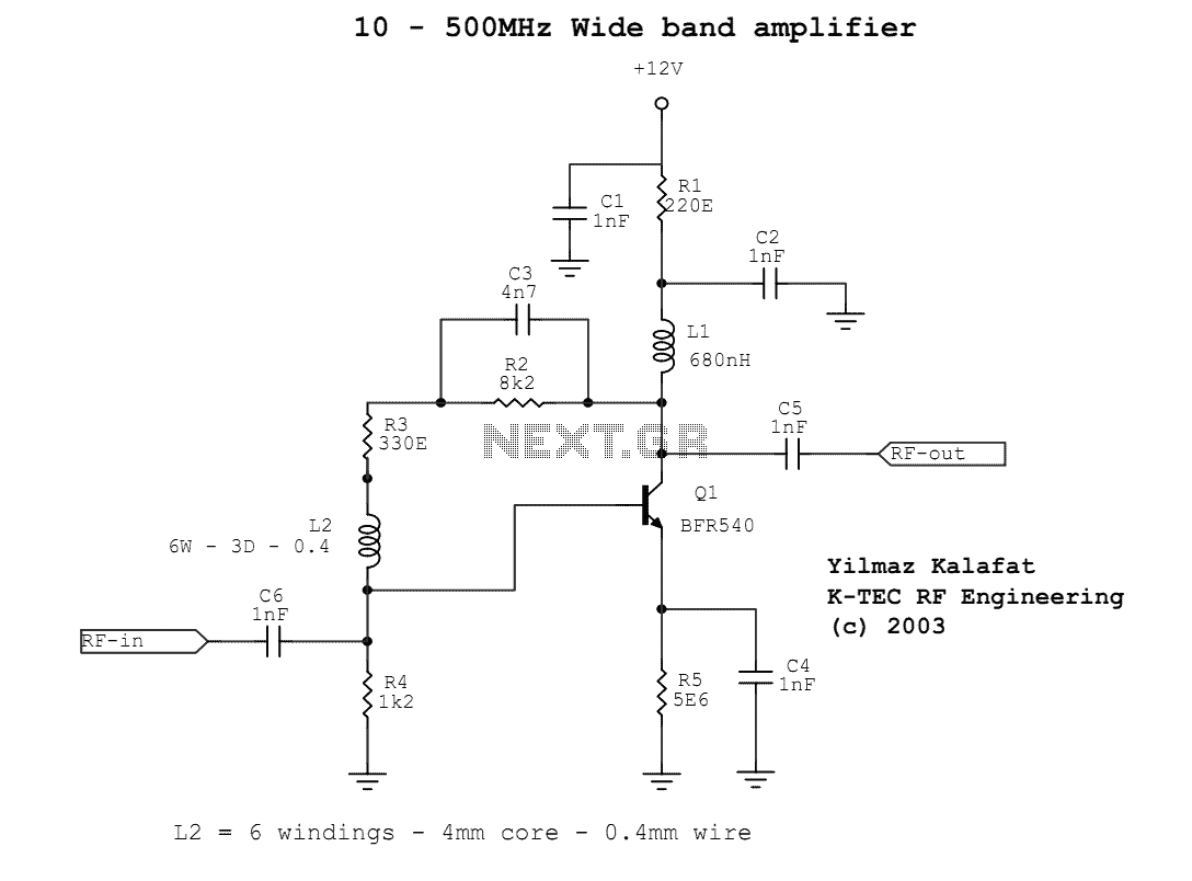
This paper describes an RF amplifier circuit which is suitable for the frequencies between 10MHz and 500MHz. These kind of amplifiers are called wide band amplifiers. Wide band amplifiers are used in communication receivers, RF measuring equipment and tons...
Figure 1 illustrates the VFO oscillator circuit operating within the frequency range of 10.58 to 10.74 MHz. This circuit is a redesigned version of a previously presented Colpitts oscillator, with a clearer representation. The inductor, labeled "L," has an...
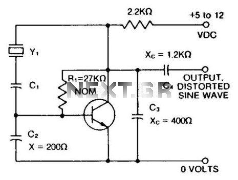
A capacitor in series with the crystal can be utilized to adjust the output frequency of the oscillator. The value can range between 20 pF and 0.01 µF, or it can be a trimmer capacitor. The values are approximate...
The schematic illustrates the division of a crystal oscillator signal by the crystal frequency to achieve a precise 1-second time base with an accuracy of 0.01%. Two cascaded 12-stage counters (CD4040) create a 24-stage binary counter, with specific bits...

The oscillator circuit employs a center-tapped transistor output transformer that functions as a load for the collector of Q1, provides a feedback signal to the base, and acts as the output winding to drive the speaker. Resistor R1 supplies...