
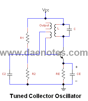
Wien Bridge Oscillator

The Wien bridge oscillator circuit consists of a configuration that includes two operational amplifiers (or transistors) arranged in a feedback loop with a Wien bridge network composed of resistors and capacitors. The R-C components are carefully selected to establish the desired oscillation frequency. The resistors R1 and R2 form the arms of the bridge, while capacitors C1 and C2 determine the phase shift characteristics. The transistors Q1 and Q2 are connected in such a way that they provide the necessary gain and phase inversion to sustain oscillations.
The circuit's stability is enhanced through the use of a thermistor or a light bulb as part of the feedback network, which adjusts the gain dynamically based on the output amplitude. This self-regulating mechanism ensures that the oscillator maintains a consistent output level, preventing distortion and frequency drift. The output can be taken from the collector of transistor Q2, providing a clean sine wave signal suitable for audio applications.
In summary, the Wien bridge oscillator is a versatile and reliable circuit used in various audio applications, characterized by its simplicity, stability, and ability to produce low-distortion waveforms over a wide frequency range. Its design allows for easy frequency adjustments while ensuring that the output remains stable and consistent.It is one of the most popular type of oscillators used in audio and sub-audio frequency ranges (20 20 kHz). This type of oscillator is simple in design, compact in size, and remarkably stable in its frequency output.
Furthermore, its output is relatively free from distortion and its fre quency can be varied easily. However, the maximum freque ncy output of a typical Wien bridge oscillator is only about 1 MHz. This is also, in fact, a phase-shift oscillator. It employs two transistors, each producing a phase shift of 180 °, and thus producing a total phase-shift of 360 ° or 0 °. It is essentially a two-stage amplifier with an R-C bridge circuit. R-C bridge circuit (Wien bridge) is a lead-lag network. The phase`-shift across the network lags with increasing frequency and leads with decreasing frequency.
By adding Wien-bridge feedback network, the oscillator becomes sensitive to a signal of only one particular frequency. This particular frequency is that at which Wien bridge is balanced and for which the phase shift is 0 °.
If the Wien-bridge feedback network is not employed and output of transistor Q2 is fedback to transistor Q1 for providing regeneration re quired for producing oscillations, the transistor Q1 will amplify signals over a wide range of frequencies and thus direct coupling would result in poor frequency stability. Thus by em ploying Wien-bridge feedback network frequency stability is increased. This bridge circuit can be used as feedback network for an oscillator, provided that the phase shift through the amplifier is zero.
This requisite condition is achieved by using a two stage amplifier, as illustrated in the figure. In this arrangement the output of the second stage is supplied back to the feedback network and the voltage across the parallel combination C2 R2 is fed to the input of the first stage. Transistor Q1 serves as an oscillator and amplifier whereas the transistor Q2 as an inverter to cause a phase shift of 180 °.
The circuit uses positive and negative feedbacks. The positive feedback is through R1 C1 R2, C2 to tran sistor Q1 and negative feedback is through the voltage divider to the input of transistor Q1. Resistors R3 and R4 are used to stabilize the amplitude of the output. The two transistors Q1 and Q2 thus cause a total phase shift of 360 ° and ensure proper positive feedback.
The negative feedback is provided in the circuit to ensure constant output over a range of frequencies. This is achieved by taking resistor R4 in the form of a tempera ture sensitive lamp, whose resistance increases with the increase in current.
In case the amplitude of the output tends to increase, more current would provide more negative feedback. Thus the output would regain its original value. A reverse action would take place in case the out put tends to fall. The above corresponds with the feedback network attenuation of 1/3. Thus, in this case, voltage gain A, must be equal to or greater than 3, to sustain oscillations. To have a voltage gain of 3 is not difficult. On the other hand, to have a gain as low as 3 may be difficult. For this reason also negative feedback is essential. The circuit is set in oscillation by any random change in base current of transistor Q1, that may be due to noise inherent in the transistor or variation in voltage of dc supply.
This variation in base current is amplified in collector circuit of transistor Q1 but with a phase-shift of 180 °. the output of transistor Q1 is fed to the base of second transistor Q2 through capacitor C4. Now a still further amplified and twice phase-reversed signal appears at the collector of the transistor Q2.
Having been inverted twice, the output signal will be in phase with the signal input to the base of transistor Q1 A part of the output signal at transistor Q2 is fedback to the input points of the bridge circuit (point A-C). A part of this feedback signal is applied to emitter resistor 🔗 External reference
Related Circuits
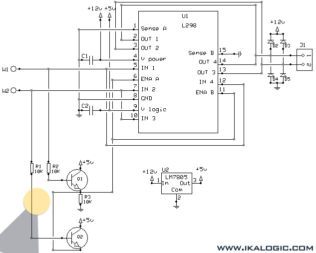
This implementation utilizes the L298 integrated circuit to drive motors and inductive loads with a continuous current capacity of up to 4A. The L298 consists of two independent channels, each capable of driving loads of up to 2A. By...
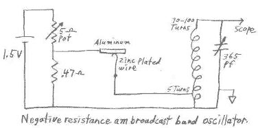
This circuit can be easily powered from a 1.5 volt battery. One characteristic of N type negative resistance devices is that they typically require a very low bias source resistance in order to keep the bias voltage stable within...
These are resonant circuits or tank circuit oscillators. They are commonly used to produce high frequencies ranging from 1 MHz to 500 MHz; hence, they are also known as RF oscillators. These oscillators are utilized in RF generators, radio...
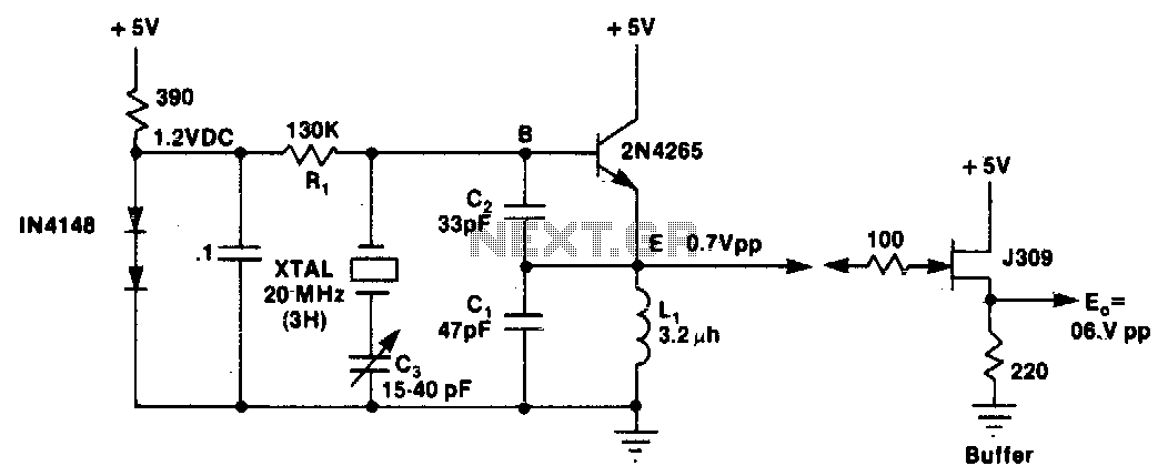
L1 and C1 are selected to resonate at a frequency below the desired crystal harmonic but above the crystal's next lower odd harmonic. Capacitor C2 should have a value between 30-70 pF, independent of the oscillation frequency. There is...
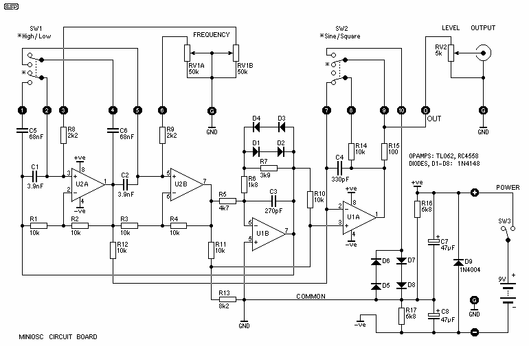
The oscillator circuit involves two unity gain phase shift stages, A1 and A2, in tandem and a gain stage, A3, with back to back diodes and resistor network providing non-linear negative feedback. At a particular frequency (determined by RT...
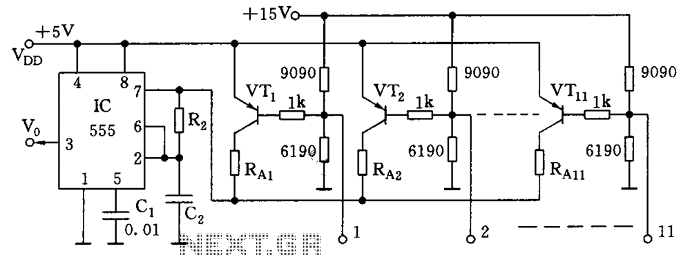
As illustrated in the figure, the base bias circuit for transistors VT1 to VT11 is designed to accept binary data, where a high level represents 1 and a low level represents 0. This configuration allows for 2048 combinations of...