
Window Comparators
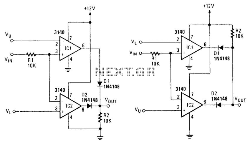
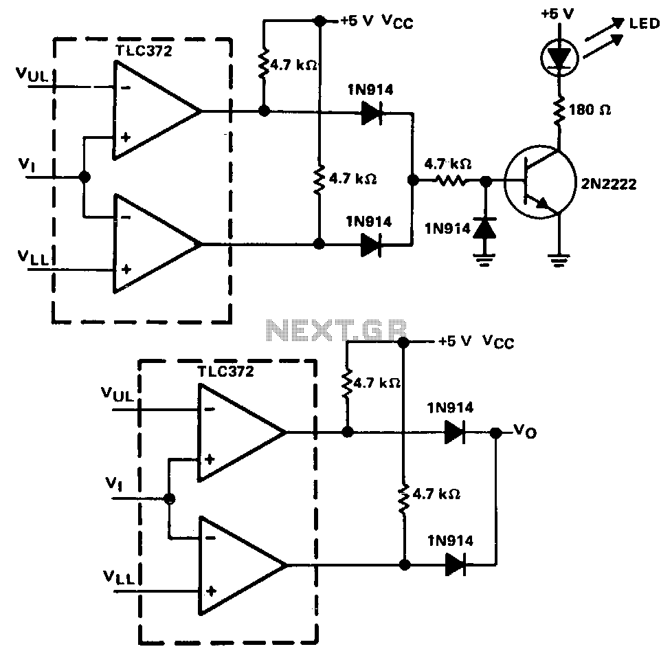
The circuit described involves two integrated circuits (IC1 and IC2) that function as voltage comparators, utilizing reference voltages to determine the output state based on the input voltage (Vin). In the configuration illustrated in Figure 104-3(a), the circuit is designed to produce a low output when Vin is within a specific range defined by the reference voltages Vi and Vu. The behavior of IC2 is particularly crucial; it generates a low signal when Vin exceeds Vl, which in turn influences the output state of the circuit.
When analyzing the conditions of the circuit, if Vin is greater than Vu, both IC1 and IC2 will output low signals, leading to a low state at Fout. This indicates that the circuit is designed to react to input voltages that exceed certain thresholds, effectively creating a logical condition that can be utilized in further electronic applications.
In contrast, Figure 104-3(b) demonstrates an alternative configuration where the circuit is designed to output a high signal when Vin is between the lower reference voltage (VL) and the upper reference voltage (Vu). This behavior highlights the versatility of the circuit design, allowing it to operate in different modes based on the input voltage levels. The use of reference voltages in this manner enables precise control over the output states, making it suitable for various applications in electronic systems where voltage thresholds are critical for operation. In Fig. 104-3(a), when Vin is between reference voltages Vi and Vu, output Vout goes low. If Vin> Vl, IC2 produces a low . Because IC1 outputs low, if V^>VUf both outputs are low and F0ut is low. If Fin < Vl, both IC1 and IC2 are low. Figure 104-3(b) operates the reverse of this; it produces a high when VL
Related Circuits
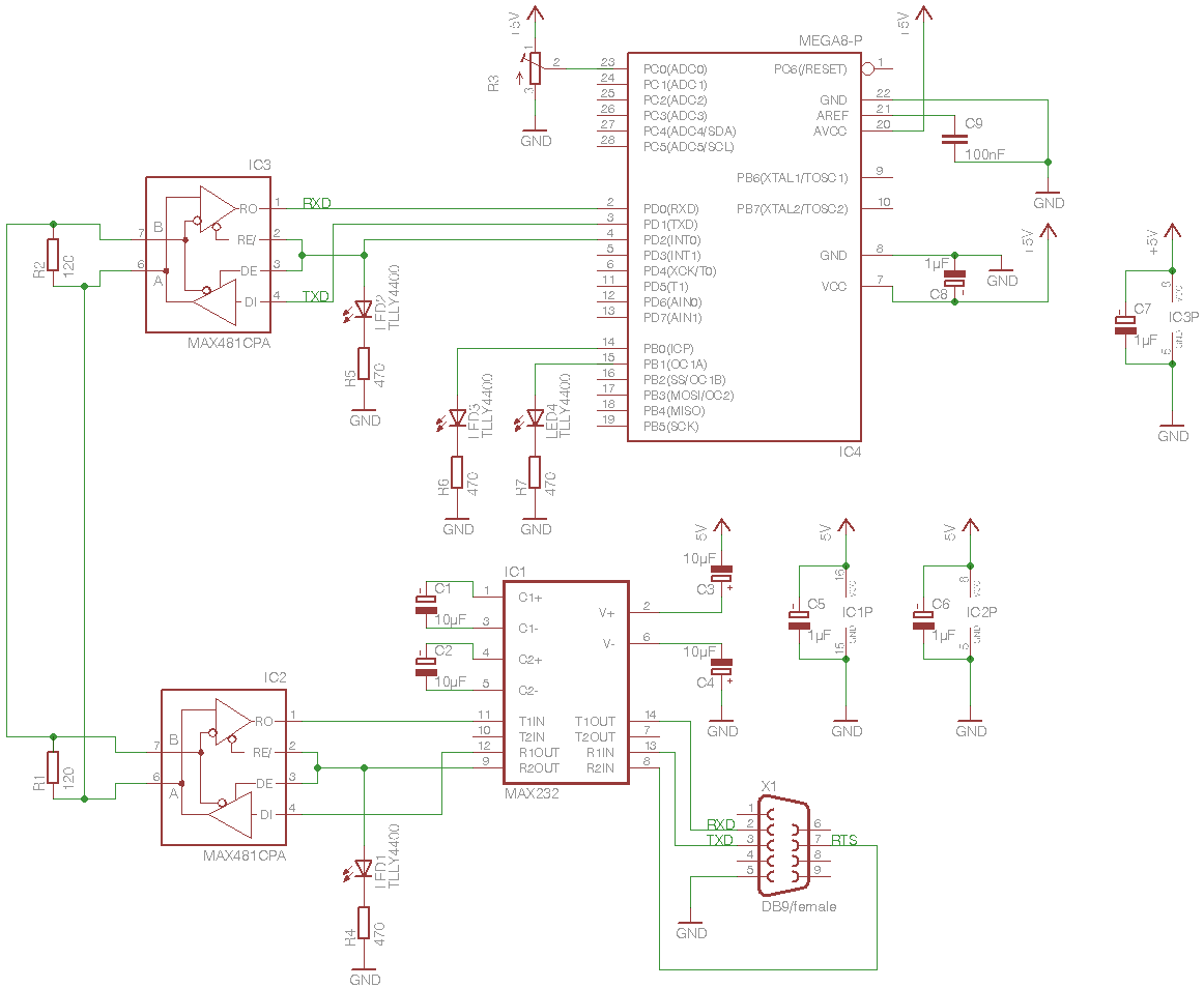
This project implements a half-duplex, master/slave communications protocol based on RS-485 bus hardware. A Windows PC acts as the bus-master, while several Atmel 8-bit AVRs function as bus-slaves. The Windows component is developed in C++, with the ninth data...
The detector circuit compares the output voltage of two separate voltage dividers with a fixed reference voltage. The resultant absolute error signal is amplified and converted to a logic signal that is TTL compatible. The described detector circuit serves as...
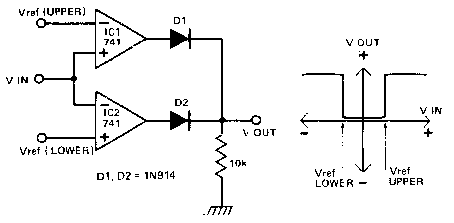
This circuit produces an output of 0V when the input voltage is within a specified range defined by two reference voltages. When the input voltage falls outside this range, the output becomes positive. Two operational amplifiers (op-amps) function as...
A window detector is a specialized comparator circuit designed to detect the presence of a voltage between two prescribed limits, which defines a voltage window. This circuit is constructed by logically combining the outputs of two single-ended comparators using...
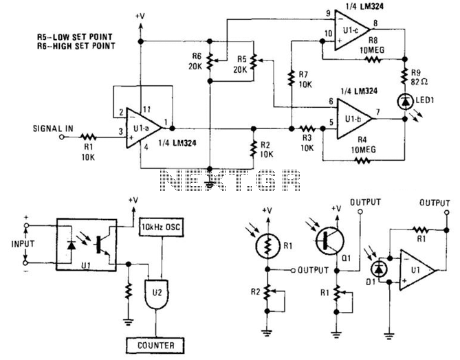
This window generator utilizes a single LM324 operational amplifier and includes two adjustable set points. When the two comparators formed by U1B go high, LED1 illuminates. When U1C goes high, the LED turns off. Hysteresis is implemented using 10...
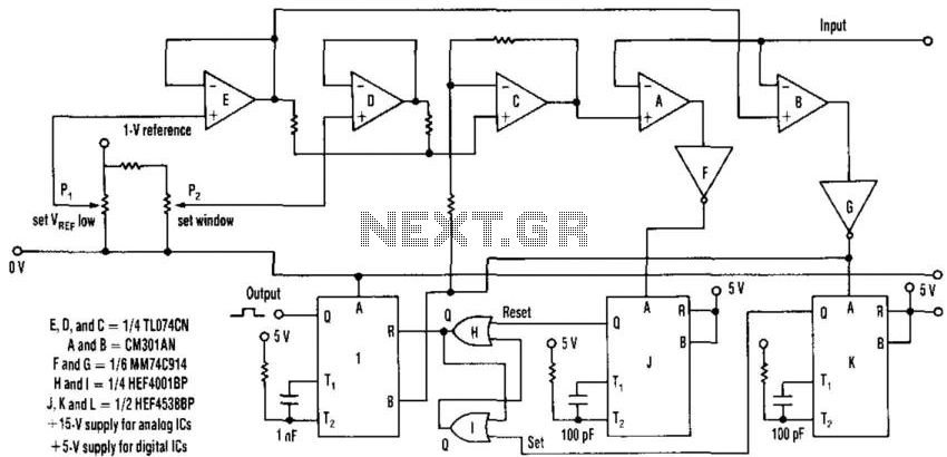
This circuit generates a TTL-compatible pulse whenever the signal falls within the limits established by the potentiometers. The circuit's configuration can be adjusted to suit specific applications. Operational amplifiers E, D, and C are utilized alongside the two potentiometers...