
Wireless two-tone electronic doorbell circuit diagram
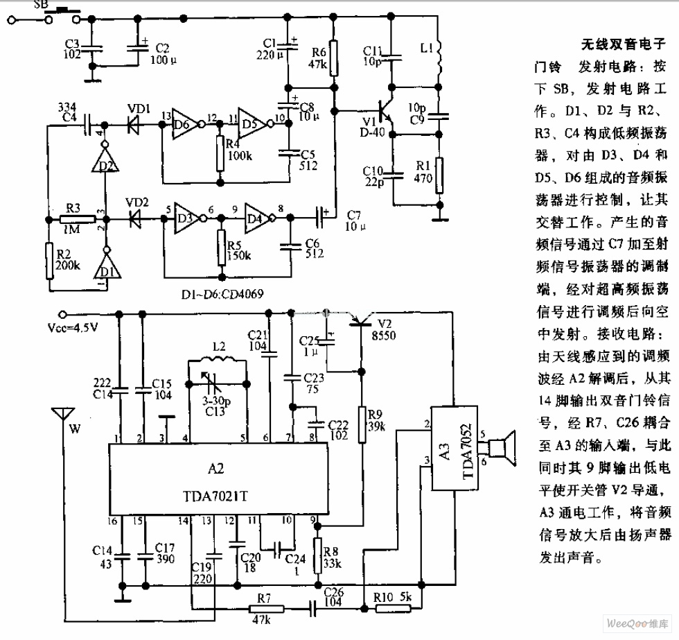
The transmitter circuit described utilizes a button switch (SB) to initiate operation. Upon activation, the circuit engages a low-frequency oscillator composed of diodes D1 and D2, along with resistors R2 and R3 and capacitor C4. This configuration generates a low-frequency signal that serves as the control mechanism for an audio oscillator, which is comprised of diodes D3, D4, D5, and D6. The alternating operation of these components allows for the modulation of the audio signal.
The audio signal produced by the audio oscillator is then introduced into the modulation side of a radio frequency (RF) signal oscillator. This integration occurs through capacitor C7, which facilitates the coupling of the audio modulation onto the RF carrier wave. The resulting high-frequency oscillator signal is then transmitted, enabling communication or signal transmission over a designated frequency range.
This circuit exemplifies a typical design used in basic transmitter applications, where low-frequency audio signals are modulated onto a higher frequency carrier for effective transmission. The careful selection of components ensures that the circuit operates efficiently, providing reliable performance in various electronic communication scenarios.Transmitter: Pressing the SB will make the transmitter circuit work. D1, D2 and R2, R3, C4 constitute a low-frequency oscillator to control the audio oscillator composed of the D3, D4 and D5, D6, then it works alternately. The generated audio signal is added to modulation side of Rf signal oscillator by C7. Then high-frequency oscillator signal is sent to ai.. 🔗 External reference
Related Circuits
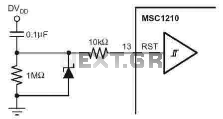
According to the MSC1210 datasheet, you will perform an external reset by taking RST pin high for two tOSC periods as this stops device operation, crystal oscillation, causes all digital pins to be pulled high from that point and...

The FAN4810 operates as a continuous conduction mode (CCM) power factor correction (PFC) controller. It features an internal safety detection mechanism that prevents circuit malfunction due to component damage. The device has a power-handling capability of up to 1A,...
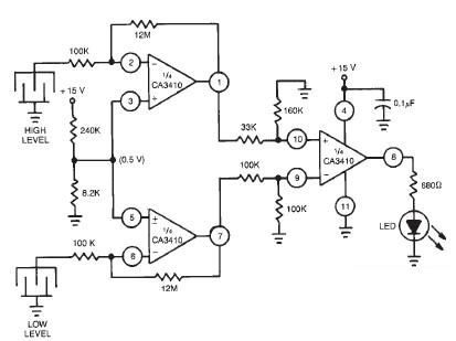
This liquid level sensor electronic circuit diagram utilizes a common CA3410 operational amplifier integrated circuit (IC). The sensor employs two plate sensors (or probes), one designated for detecting high liquid levels and the other for low liquid levels. If...
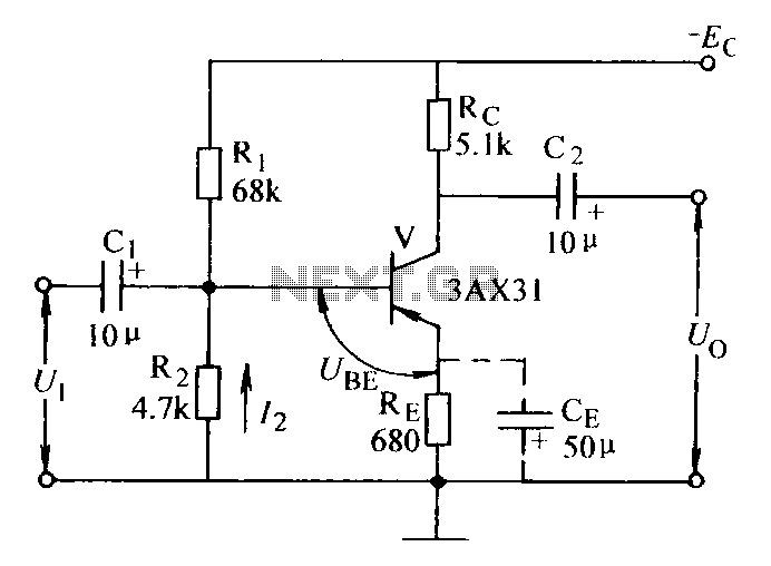
Current negative feedback voltage divider biased circuit diagram. The current negative feedback voltage divider biased circuit is a configuration commonly used in electronic amplifiers to stabilize the operating point and improve linearity. This circuit typically consists of an amplifier, a...
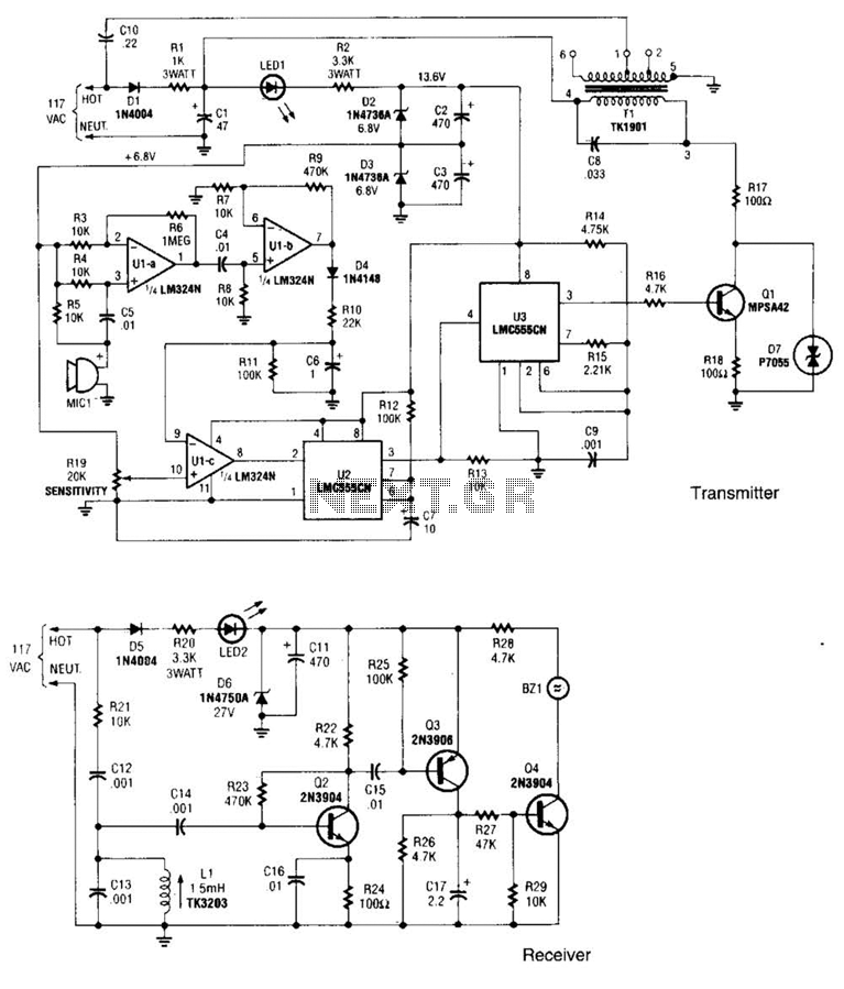
The transmitter operates by deriving its power directly from the AC line. The DC power required for the circuit is generated in two stages: the first stage powers the RF power amplifier, while the second stage supplies power to...
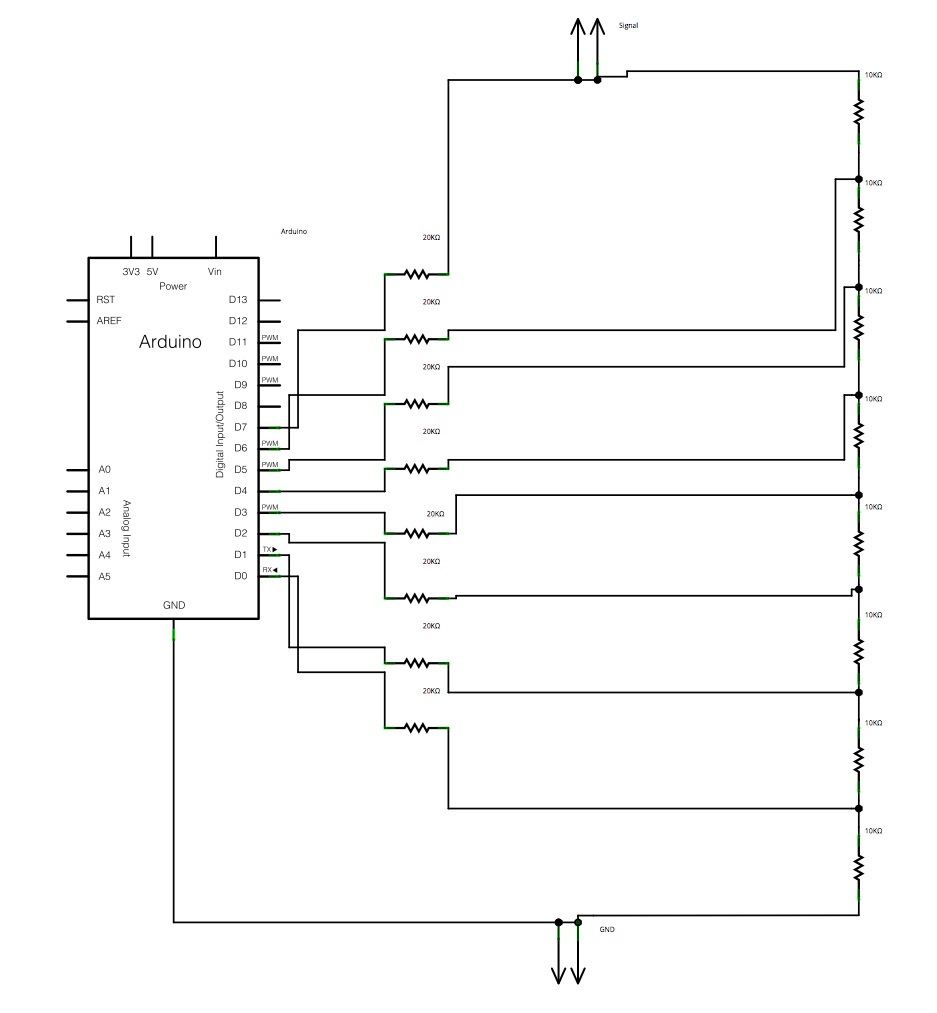
The main concept is to space the time intervals to increment the DAC output values. There are 256 levels since there are 8 digital outputs from the Arduino board. Therefore, for an 8-bit resolution and a 50-second ramp time,...