
Zero crossing switch
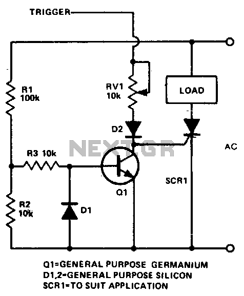
The described circuit serves as an effective solution to mitigate RFI when controlling loads with a thyristor. The use of a single transistor as a zero crossing switch allows for precise timing in the conduction of the thyristor, ensuring that it only activates when the AC voltage crosses zero, thus minimizing the abrupt changes in current that contribute to RFI.
In this configuration, resistors R1 and R2 create a voltage divider that scales down the AC voltage to a manageable level for the transistor's base. The junction voltage, being around 10% of the AC voltage, ensures that the transistor remains in an off state until the AC waveform approaches zero, at which point the voltage rises enough to turn on the transistor.
Resistor R3 plays a crucial role by providing a current path to the base of the transistor, allowing it to switch on and effectively shunt the thyristor gate current to ground. This action is essential for controlling the thyristor's operation, preventing unintentional triggering and ensuring that the thyristor only conducts when intended.
Diode D1 is strategically placed to protect the circuit from negative voltages that could otherwise cause damage to the thyristor. By blocking any reverse voltage, D1 ensures the reliability and longevity of the circuit components.
Overall, this simple yet effective design illustrates the importance of zero crossing detection in thyristor applications, enhancing performance while reducing unwanted electromagnetic interference.When switching loads with the aid of a thyristor, a large amount of RFI can be generated unless some form of zero crossing switch is used. The circuit shows a simple single transistor zero crossing switch. Rl and R2 act as a potential divider. The potential at their junction is about 10% of the ac voltage. This voltage level is fed, via R3, to the transistor"s base. If the voltage at this point is above 0, the transistor will conduct, shunting any thyristor gate current to ground
When the line potential is less than about 2 V, it is possible to trigger the thyristor. The diode Dl is to remove any negative potential that might cause reverse breakdown. 🔗 External reference
Related Circuits
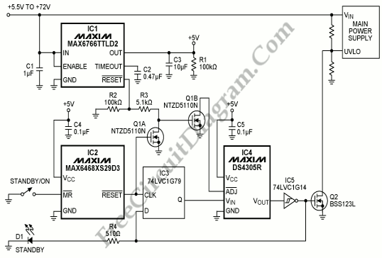
The STANDBY/ON switch is suitable for applications such as industrial and telecom, where the circuitry needs to retain its state (either STANDBY or ON). The STANDBY/ON switch circuit is designed to maintain the operational state of the system, ensuring that...
A DC-to-DC step-up converter is typically implemented using a transformer, which converts DC voltage to AC voltage, steps it up with the transformer, and then rectifies and filters the output to achieve a higher DC voltage. However, a voltage...

This circuit utilizes a tachometer to generate a feedback signal that is compared to a reference provided by the auxiliary output. Upon power application, the tachometer output is initially zero, allowing the regulator output to activate and supply current...
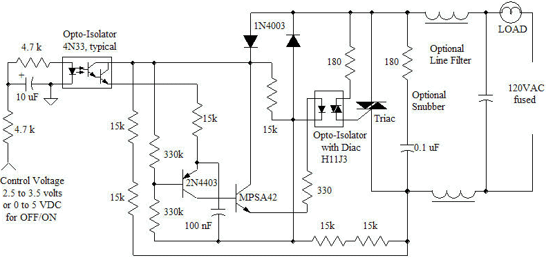
This line voltage power controller connects a DC control voltage or microprocessor logic output to an AC load. By adding a filter capacitor to the input resistors, the circuit can be controlled by a duty-cycle modulated square wave with...
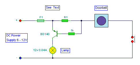
This circuit activates a lamp at a remote location when the doorbell switch is pressed. It is designed specifically for solenoid-type doorbells, as electronic doorbells that play tunes are incompatible. The circuit addresses the issue of potentially missing the...
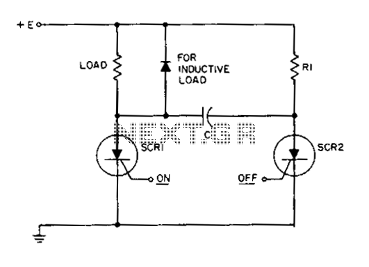
This circuit is a static SCR switch designed for use in a DC circuit. When a low-power signal is applied to the gate of SCR1, this SCR is triggered, allowing voltage to be applied to the load. The right...
Warning: include(partials/cookie-banner.php): Failed to open stream: Permission denied in /var/www/html/nextgr/view-circuit.php on line 713
Warning: include(): Failed opening 'partials/cookie-banner.php' for inclusion (include_path='.:/usr/share/php') in /var/www/html/nextgr/view-circuit.php on line 713