
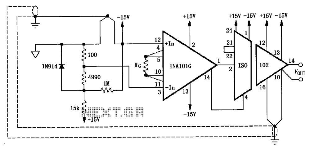
Basic circuit diagram connection of signal and power ISO107

The ISO107 is an isolated signal and power supply interface that requires careful attention to bypassing and load connections to ensure optimal performance. Each power supply terminal must be equipped with a bypass filter to stabilize the voltage and reduce noise. For applications where the output current exceeds 15 mA, an external filter should be connected to the +Vcc2 pin to enhance the power supply's stability. The suggested values for the inductor (Lo) at 10 µH and capacitor (Co) ranging from 0.1 µF to 10 pF are critical for filtering high-frequency noise and maintaining signal integrity.
In the schematic, Com1 serves as the connection point to the signal source, while Com2 connects to the load (RL). The Sense line is strategically placed at the upper end of the load to mitigate the impact of voltage drops that can occur due to long wire lengths. This configuration helps maintain accurate voltage readings and enhances the overall reliability of the circuit. Ground connections are also essential; Gnd1 is linked to Com1, and Gnd2 is connected to Com2, ensuring a common reference point for the circuit.
The output voltage sensing (Vout Sense) and the photogenic receptacle connector are integrated into the design, allowing for easy interfacing with external devices. Proper layout and component selection are vital to minimize parasitic inductance and capacitance, which can adversely affect the performance of the ISO107 circuit. Overall, this configuration provides a robust solution for isolated signal and power supply applications, ensuring minimal interference and maximum efficiency. As shown for the basic connection circuit ISO107 signal and power supply. Each power supply terminal must have a bypass filter. When isolated power supply output current is gre ater than 15mA, we recommend the use of such power pin of + Vcc2 pin external filter. Lo 10 H, Co is 0.1 ~ 10pF. Com1 feet to the signal source, Com2 connected to load RL, Sense then load the upper end, in order to reduce errors due to long wires cause a voltage drop caused by the transmission. Gnd1 connected to Com1, Gnd2 and Com2 connected, Vout Sense and photogenic receptacle connector.
Related Circuits
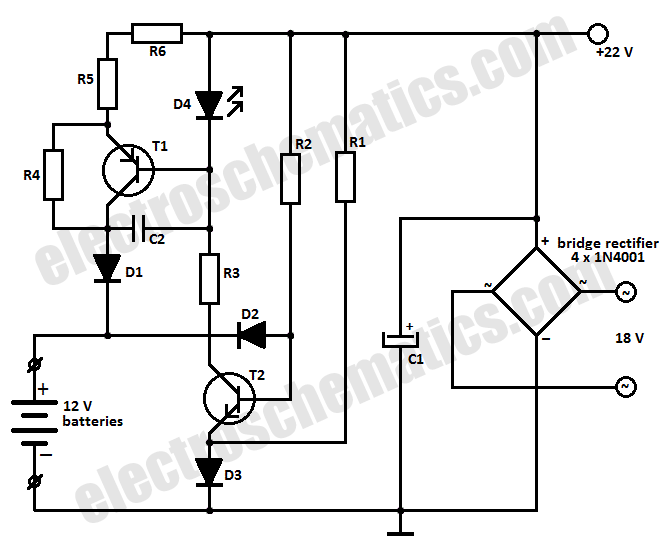
This battery charger circuit is designed to charge one or more batteries with a total nominal voltage of 12 V, which accommodates either ten NiCd batteries or six 2 V lead-acid batteries. The battery charger circuit operates by utilizing a...
This circuit was originally a type of power-delay control circuit, where the delay time is determined by the timing elements R1 and C1. Additionally, with the inclusion of a "watchdog" circuit, it can be utilized as a monitoring circuit...

The common characteristic of all previous low-power FM transmitters built over the decades is that their operating frequency is determined by an LC resonant circuit. Some of these transmitters exhibited excellent stability, while others did not; however, there has...
If the audio input is a microphone, it is expected to precede an amplifier to achieve an output power of approximately 8W. The amateur seeking to enhance a small transmitter, which is likely already constructed, can utilize this circuit,...
The circuit, as illustrated in the figure, consists of an ISO102 and an INA101 designed to eliminate ground loops and provide high-end cold junction compensation for a thermocouple amplifier. This configuration utilizes a K-type thermocouple to detect temperature at...
This is a cost-effective circuit that incorporates precise current limiting functionality into a voltage regulator. The circuit described is designed to enhance the performance of a voltage regulator by integrating a current limiting feature. This is particularly beneficial in applications...