
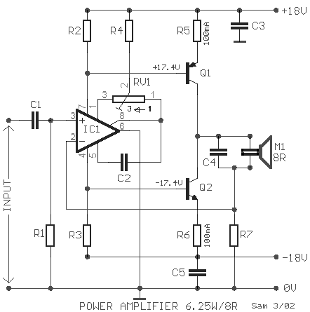
1 Watt 2.3 ghz amplifier

The networks are engineered to deliver approximately 3% 1 dB power bandwidth while achieving a collector efficiency of around 30%. One tuning adjustment is present in the amplifier, specifically at Cl in the output network. Ceramic chip capacitors, designated as C2 and C3, are employed for DC blocking and power supply decoupling, while additional low-frequency decoupling is facilitated by capacitors C4 and C5.
This 1-watt S-band amplifier design is characterized by its efficient use of the MRF2001 transistor in a common base configuration, which is well-suited for Class C operation. The amplifier's ability to deliver a minimum gain of 8 dB at a supply voltage of 24 V is indicative of its robust performance in the specified frequency range of 2.25 to 2.35 GHz. The design is particularly advantageous for applications requiring narrowband amplification, such as in microwave communication systems.
The use of distributed microstrip elements in the circuitry enhances the amplifier's performance by minimizing losses and optimizing the signal integrity across the operational bandwidth. The design's impedance matching to 50 ohms through double-section low-pass networks is crucial for ensuring maximum power transfer and minimizing reflections, which is essential in high-frequency applications.
The bandwidth specification of approximately 3% for the 1 dB power bandwidth indicates the amplifier's capability to maintain consistent performance across a defined frequency range. The choice of a collector efficiency of around 30% reflects a balanced approach between power output and thermal management, which is critical in maintaining the reliability of the amplifier during extended operation.
The tuning capability provided by the adjustment at Cl in the output network allows for fine-tuning of the amplifier's performance, accommodating variations in component tolerances and environmental conditions. The inclusion of ceramic chip capacitors for DC blocking and power supply decoupling (C2 and C3) ensures that the amplifier operates efficiently without unwanted DC offsets or noise. Furthermore, the additional low-frequency decoupling capacitors (C4 and C5) serve to enhance power stability, reducing the risk of oscillations and ensuring that the amplifier maintains its performance characteristics under varying load conditions.
Overall, this amplifier design exemplifies a well-engineered solution for medium power applications in the S-band, combining effective component selection with thoughtful circuit design to achieve desirable performance metrics.Simplicity and repeatability are featured in this 1 watt S-band amplifier design. The design uses an MRF2001 transistor as a common base, Class C amplifier. The amplifier delivers 1 watt output with 8 dB minimum gain at 24 V, and is tunable from 2.25 to 2.35 GHz. Applications include microwave communications equipment and other systems requiring medium power, narrow band amplification.
The amplifier circuitry consists almost entirely of distributed microstrip elements. A total of six additional components, including the MRF2001, are required to build a working amplifier. The input and output impedances of the transistor are matched to 50 ohms by double section low pass networks.
The networks are designed to provide about 3% 1 dB power bandwidth while maintaining a collector efficiency of approximately 30%. There is one tuning adjustment in the amplifier—Cl in the output network. Ceramic chip capacitors, C2 and C3, are used for dc blocking and power supply decoupling. Additional low frequency decoupling is provided by capacitors C4 and C5.
Related Circuits
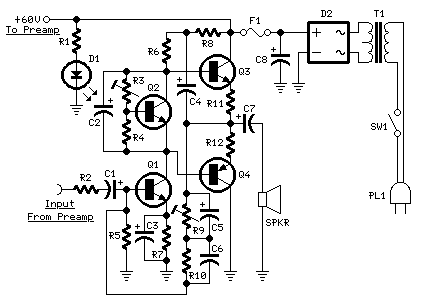
This design utilizes a well-established circuit topology for the power amplifier, employing a single-rail supply of approximately 60V and capacitor coupling for the speakers. The advantages of this configuration for a guitar amplifier include a straightforward circuit design, even...
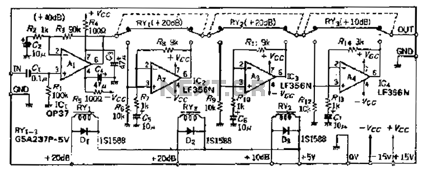
Although the basic amplifier circuit phase AC amplifier remains unchanged, the selection of the correct gain requires the use of series resistors. The circuit does not include a 9kΩ resistor. The input amplifier Ai selected is the OP37, which...
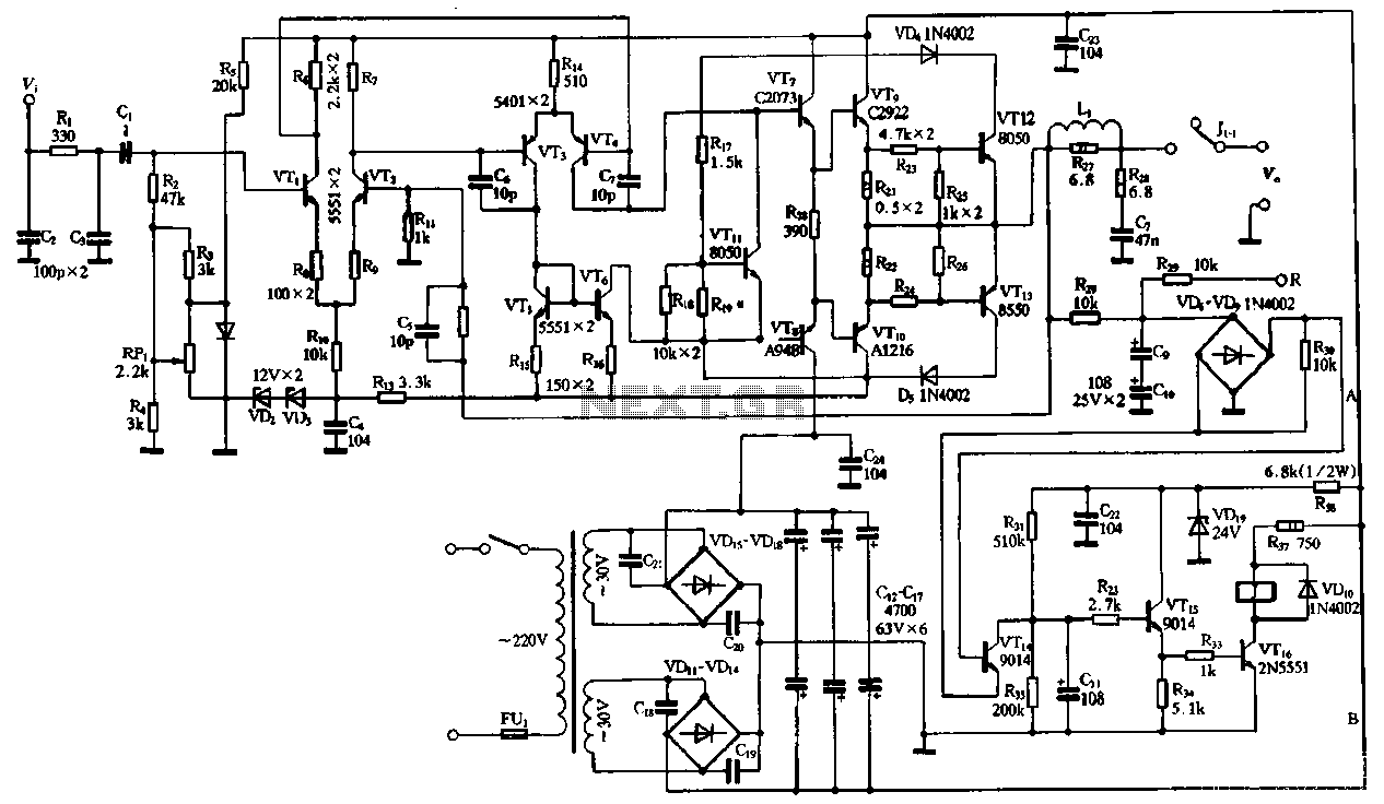
The performance of the amplifiers 2SC2922 and 2SA1216 (or 2SC3264 and 2SA1295) is excellent, featuring good linearity and strong overload capabilities. These devices are utilized as high-fidelity power amplifier stages, demonstrating outstanding performance. The circuit, as illustrated in Figure...

A careful examination of the amplifier photos reveals that the heatsink on the HY60 near-clone built using the TDA2050A is slightly shorter than that of the original HY60s. This unit is positioned at the rear of the amplifier, creating...
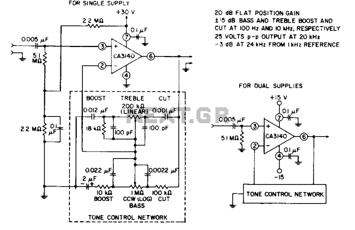
The circuit effectively utilizes the high slew rate, wide bandwidth, high input impedance, and high output voltage capability of the CA3140 BiMOS operational amplifier. The wideband gain of this circuit is equal to the ultimate boost or cut plus...
The amplifier circuit utilizes negative current feedback, which ensures that the load current is primarily influenced by the input signal rather than the loudspeaker's impedance. The inductor current from the loudspeaker generates a voltage across resistor R7, which is...