
An op-amp made from 555 chips

To address this, a different approach can be taken: utilize two 555 timers, one for each input of the op-amp, and employ the high-impedance threshold pin on each 555 to compare the inputs against a common ramp generated by an auxiliary 555 timer. This method converts voltage to time and uses additional logic (implemented with 555 timers) to compare the PWM signals, generate error pulses, and integrate them. The schematic illustrates one possible implementation using the TS555 from ST Microelectronics, a CMOS 555 with enhanced specifications compared to the original bipolar version. Initially, a conventional astable oscillator generates a sawtooth waveform oscillating between 1/3 Vcc and 2/3 Vcc. This waveform is fed into the control inputs of two additional 555 timers, which function as analog comparators, producing PWM waveforms that represent the op-amp input voltages. Digital gates, also constructed with 555 timers, compare the edges of the PWM signals, generating pulses when waveform A leads or lags behind waveform B. These generated pulses are then integrated using a capacitor, with diodes employed to isolate the two totem-pole outputs. In total, ten 555 timers are utilized in this design.
This configuration resembles a charge-pump phase-locked loop (PLL). Initially, the circuit was constructed without the inverter pairs, leading to unstable behavior characterized by hysteresis and distorted waveforms. This instability arises because, at equilibrium, the edges of the signals are closely spaced, preventing the gates from producing sufficiently narrow pulses to accurately reflect small phase differences. The solution employed mirrors techniques used in PLL circuits: anti-backlash delays. The introduction of inverter pairs creates sufficient delay, ensuring that at equilibrium, pulses are generated in both the positive and negative paths, which cancel upon reaching the integrating capacitor. Consequently, minor movements in the PWM edges result in a linear net charge to the capacitor. An alternative op-amp implementation could involve voltage-to-frequency converters at the inputs, followed by frequency comparisons using a sequential phase-frequency detector, also constructed with 555 timers. However, this method is more complex and raises concerns about injection locking, leading to the decision not to pursue it further.Is it possible to make an op-amp out of nothing but 555 chips and passive components? Not a terribly practical question, given the existence of very inexpensive and capable op-amps covering every corner of op-amp performance space; but it has some aesthetic appeal. If you find yourself on a desert island with nothing but a pile of 555s and a need for an op-amp, by all means read on.
The 555 has two comparators, but offers direct access to neither. The "trigger" comparator could conceivably work with feedback from the control pin, but the existence of a 2:1 resistive divider in the feedback path is very awkward. And while the "threshold" comparator sees both the input pin and the control pin directly, unfortunately its output can't flow through the digital portion of the 555: the threshold comparator can only reset the RS latch, not set it.
Even if we could use the threshold or trigger comparators directly, they have the disadvantage that one of their inputs is tied to a resistive bias network, resulting in a very low input impedance on that input (in the neighborhood of 30k ohm for the CMOS flavors of the 555; 3k ohm for bipolar). Potentially tolerable for something like a unity-gain buffer, where a low-impedance output drives the input pin, but not good for a general-purpose op-amp.
So instead we can adopt the following approach: use two 555s, one for each op-amp input, using the high-z threshold pin on each 555 compare the inputs to a common ramp generated by an auxiliary 555, converting voltage to time use postprocessing logic (implemented with "555 gates") to compare the PWM signals, generate error pulses, and integrate them The schematic below shows one implementation. I used the TS555 from ST Microelectronics; it is a CMOS 555 with improved specs over the bipolar original.
First, a conventional astable oscillator generates a sawtooth waveform ranging between 1/3 Vcc and 2/3 Vcc. This is fed to the control inputs of two additional 555 chips serving as analog comparators; their outputs encode the op-amp input voltages as PWM waveforms.
The digital gates (implemented with 555 chips, of course, as shown at the bottom of the schematic) compare the edges of the PWM waveforms, generating pulses if waveform A is ahead of waveform B or vice-versa. These pulses are integrated with a capacitor, using diodes to isolate the two totem-pole outputs (I suppose one could dispense with the lower diode and use the open-drain 555 pin instead).
Ten 555 chips are used in all. This is all quite similar to a charge-pump PLL. In fact I built the circuit first without the inverter pairs and wound up with some flaky behavior: hysteresis, distorted waveforms, etc. This is because at equilibrium the edges are very close together and the gates cannot generate pulses narrow enough to represent the tiny phase difference.
The solution is the same one the PLL chips use: anti-backlash delays. The inverter pairs introduce enough delay so that at equilibrium, pulses are generated in both plus and minus arms, which cancel once they hit the integrating capacitor. And now small PWM edge movements result in linear net charge to the capacitor. Speaking of PLLs, another possible op-amp implementation would use voltage-to-frequency converters at the inputs, then compare the frequencies with a sequential ("type-IV") phase-frequency detector, again implemented with 555 chips.
But besides being more complicated, one might worry about injection locking. I ended up not trying it.
Related Circuits

The circuit illustrated briefly flashes an LED to attract attention and remains illuminated as long as power is supplied. The circuit utilizes the well-known 555 timer integrated circuit (IC) configured as a standard astable multivibrator with resistors RA, RB,...
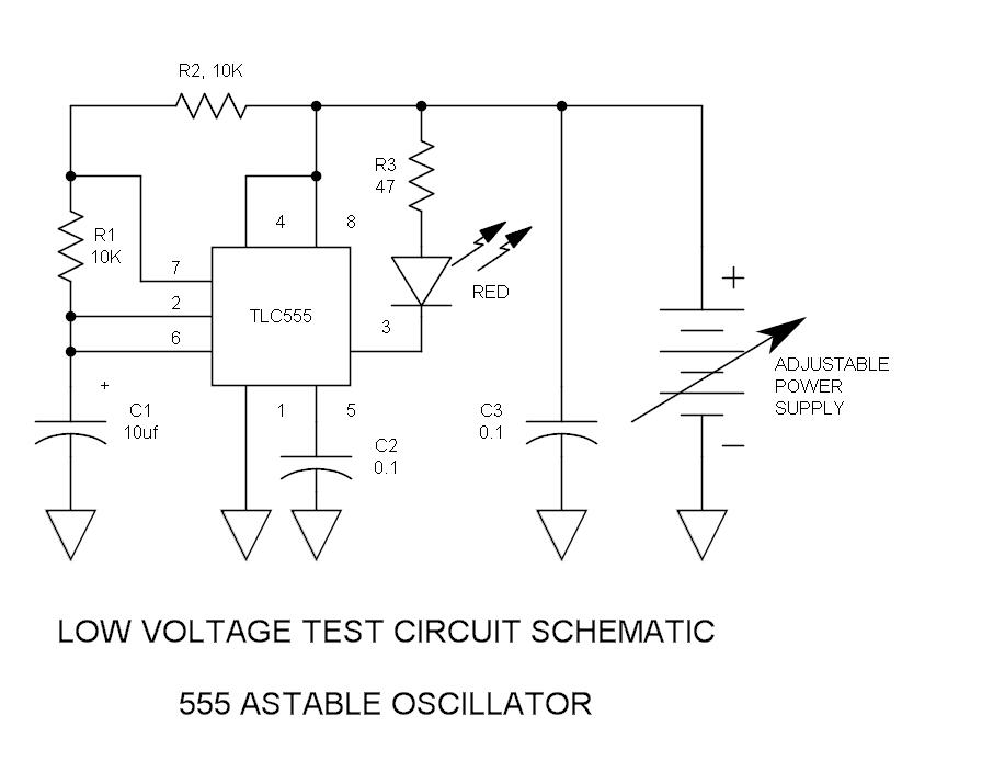
There have been stories regarding the suboptimal performance of the 555 timer IC when operated below a supply voltage (Vcc) of 5V, prompting an investigation into potential improvements for its operation. The 555 timer IC is a versatile device commonly...

The circuit is a direct-reading frequency meter that utilizes an amplifier and a one-shot trigger circuit, along with table-top components. It is capable of directly detecting a 1mA signal at the read head, with a maximum signal frequency of...

This 555 timer circuit below toggles a relay when a button is pressed. Pins 2 and 6, the threshold and trigger inputs, are held at 1/2 the supply voltage by the two 10K resistors. When the output is high,...
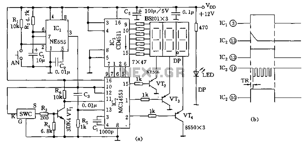
The digital thermometer consists of a temperature sensor, a single stabilizing circuit, a counter circuit, a decoding section, a driving circuit, and LED digital tubes among other components. It operates within a temperature range of 0 to 50 degrees...
A mechanical engineering student is designing a project that requires a timer to switch off a motor approximately 40-50 seconds after activation. The student references the 555 timer chip, indicating that the chip has a rectangular shape with an...