
Mono to stereo circuit

This circuit appears to describe a variable output voltage system, likely utilizing a potentiometer or a similar adjustable component. The output voltage is dependent on the input voltage (Vin) and varies based on the position of the adjustable component.
At the center position of the potentiometer, the output voltage is calculated to be 0.707 times the input voltage, indicating a specific attenuation of the signal. This could suggest that the circuit is designed to provide a stable reference voltage or a specific gain setting, often utilized in audio applications or signal processing where a controlled output is necessary.
At the extreme positions of the adjustable component, the output voltage equals the input voltage (Vin), allowing for full signal transmission without attenuation. This functionality indicates that the circuit is capable of operating as a variable gain amplifier or a voltage divider, depending on the configuration of the components in the circuit.
The overall design likely includes additional components such as resistors or capacitors to stabilize the output and prevent noise, ensuring that the voltage output remains consistent across the varying positions of the adjustable component. The circuit may also incorporate feedback mechanisms to enhance performance and linearity across the entire range of operation.
In summary, the described circuit is a versatile voltage output system, capable of providing both attenuated and full output levels based on the position of the adjustable component, making it suitable for applications requiring precise voltage control.The output voltage is = 0.707 x Vin, at the center posititon. The output voltage is = Vin, at either extreme position. 🔗 External reference
Related Circuits
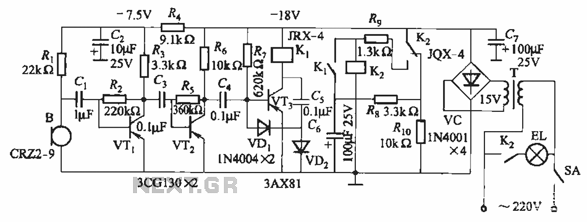
The circuit utilizes relay control. The voice switch operates as follows: upon the first clap, the load (lights) is activated; upon the second clap, the load (lights) is deactivated. This system can be employed to control lighting in residential...
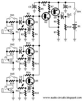
The following circuit illustrates a Mini Audio Mixer with Level Control Circuits. Features include switchable high/low sensitivity, providing high performance. The Mini Audio Mixer circuit is designed to facilitate the mixing of multiple audio signals while allowing for level control...
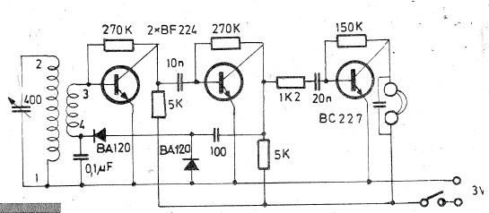
Oscillating circuits (coils) are constructed on a ferrite bar. For long wave reception, winding "1-2" consists of 135 turns, while winding "3-4" consists of 20 turns. For medium wave reception, winding "1-2" has 75 turns, and winding "3-4" has...
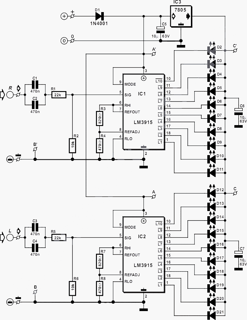
This circuit detects the AC audio voltage supplied to car radio loudspeakers and visually represents it as power using an LED bar graph, creating an appealing visual effect. It is designed to accommodate typical car radio output power ranges...
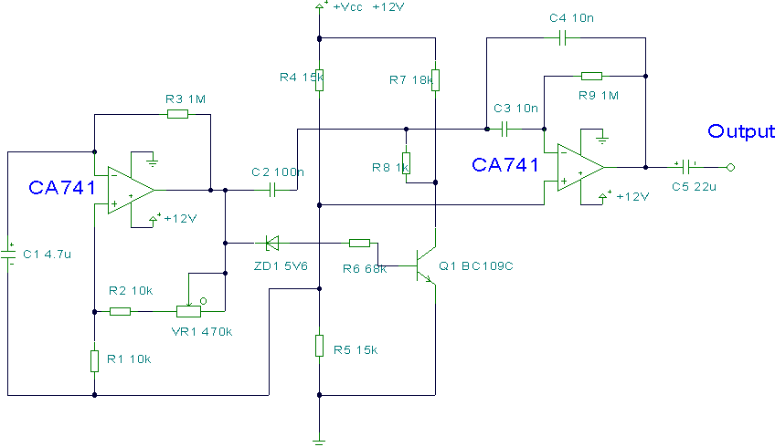
This circuit utilizes two operational amplifiers (op-amps) to create a unique sound effect. The first op-amp, CA741, is configured as a standard astable multivibrator, generating timing pulses controlled by components C1, R2, and variable resistor VR1. The output from...

This device offers numerous implementation possibilities due to its wide input voltage range and large maximum output current across a broad output voltage spectrum. It features long battery life and low power consumption owing to its high efficiency and...