
Logic Circuits Vs Transistor Power Circuits
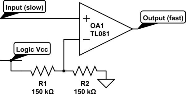
To achieve the goal of inverting a signal for driving FETs with fast rise and fall times, a discrete inverter circuit can be constructed using a combination of transistors. This design allows for greater control over the switching characteristics compared to standard logic chips. The key components in this circuit include a bipolar junction transistor (BJT) or a MOSFET configured as a NOT gate.
The basic operation involves using a resistor to pull the base of the BJT high when the 555 timer output is low, turning the transistor ON, which in turn pulls the output low. Conversely, when the 555 timer output is high, the transistor is turned OFF, allowing the output to rise. The choice of resistor values and the transistor type will significantly affect the rise and fall times of the output signal. It is essential to select a transistor with a suitable switching speed and ensure that the pull-up resistor is appropriately sized to achieve the desired performance.
When implementing this circuit, several considerations must be taken into account. The power supply voltage and current ratings of the FET being driven must be compatible with the output characteristics of the inverter circuit. Additionally, the layout of the circuit should minimize parasitic capacitance and inductance to ensure fast switching times. Proper decoupling capacitors should be placed near the power supply pins of the 555 timer and the inverter circuit to prevent voltage dips during switching.
Furthermore, it is crucial to understand the input and output impedance characteristics of the 555 timer and the inverter circuit. The output of the 555 timer should be capable of driving the base or gate of the inverter transistor without significant voltage drop. It may be beneficial to simulate the circuit using software tools to evaluate performance before physical implementation, ensuring that the desired switching characteristics are met.
In summary, building a discrete inverter circuit with careful attention to component selection and circuit layout will enable effective signal inversion for driving FETs. Understanding the nuances of logic circuitry and the specific requirements of the components involved will enhance the reliability and performance of the final application.Invert a signal to drive fets with hard/fast rise and fall times. I was told in another thread to use an inverter (NOT chip). This makes perfect sense to me since logic chips are always hard ON or OFF by design. But I`ve never worked with logic chips before. All I`ve dealt with is 555s and transistor/fet power circuits. Are there any `gotchas` or special things I need to know to implement a NOT chip into a 555 output to switch a FET without any hiccups For that matter, are there any `gotches` or things in general that apply to logic circuitry that someone with my background wouldn`t know and might stumble on 🔗 External reference
Related Circuits
This project is designed to charge a pair of AA Nickel Metal Hydride (NiMH) or Nickel Cadmium (NiCd) cells using a laptop's USB port for power. It addresses the need for a convenient charging solution. Any USB port can...
Figure 1 illustrates an AND gate logic circuit with the logic expression P=A. Figure B depicts two photodiodes connected in series. When the input logic levels A=1 and B=1, the output P=1. Similarly, this configuration can be used to...

Darlington phototransistor type light-sensitive switch control circuit application. The Darlington type phototransistor serves as a sensitive element, capable of detecting low light levels for the detection of reflected light signals. The Darlington phototransistor circuit utilizes a pair of transistors configured...
The simple zener shunt in configuration A may not handle sufficient current if the zener diode available is of low wattage. A power transistor will perform most of the work for the zener as illustrated in configuration B. Once...

Most power supplies regulate either their output voltage or current at a constant level, depending on the load resistance relative to the power supply's output voltage and current settings. This can be summarized as follows: To accomplish this, most...
Power outages following a call prevent the re-closure of a circuit, which can help avoid the use of electrical appliances after the power grid is restored. If appliances are left on and a call occurs, it may lead to...