
electrical engineering logic gates

The circuit design involves four single-bit inputs labeled X, Y, T, and Z, and a single-bit output designated as E. The selection of the input to be propagated to the output is controlled by a two-bit control code, S0S1, where S0 represents the least significant bit and S1 represents the most significant bit. The control codes correspond to the binary values that select one of the four inputs, as follows:
- S0S1 = 00 selects input X
- S0S1 = 01 selects input Y
- S0S1 = 10 selects input T
- S0S1 = 11 selects input Z
To implement this selection mechanism, a multiplexer (MUX) can be used, which is a standard combinatorial logic circuit. A 4-to-1 multiplexer is suitable for this application, as it can take four inputs and select one based on the state of the two control bits.
The circuit diagram would illustrate the four inputs connected to the multiplexer, with the outputs of the multiplexer connected to the output E. The control inputs S0 and S1 would be connected to the select lines of the multiplexer.
In terms of logic gates, the multiplexer can be constructed using AND, OR, and NOT gates. Each input can be ANDed with a corresponding select line combination that allows it through to the output, and the results of these AND gates can be combined using an OR gate to produce the final output E.
The truth table for the circuit will clearly show the relationship between the control codes and the selected inputs:
| S1 | S0 | Output E |
|----|----|----------|
| 0 | 0 | X |
| 0 | 1 | Y |
| 1 | 0 | T |
| 1 | 1 | Z |
This table summarizes the functionality of the circuit, ensuring that the correct input is routed to the output based on the selected control code. The design can be implemented on a breadboard or within a simulation environment to validate its operation.Design a circuit with four single-bit inputs X, Y, T, and Z, but only one single-bit output E. A two bit control code word S0S1 selects which of the four inputs is propagated to the output (the selection code is not unique). Your answer should be in the form of a circuit diagram and table showing which selection code selects which input.
You may use any of the combinatorial logic gates.. 🔗 External reference
Related Circuits
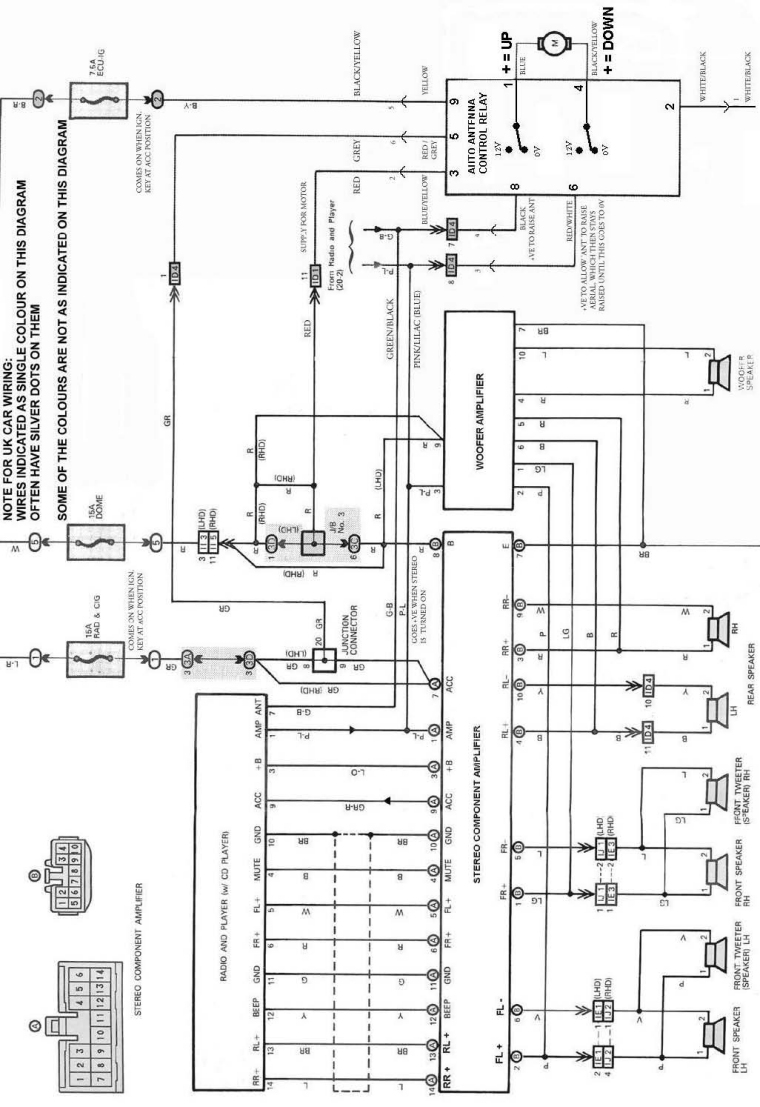
The following circuit illustrates an electrical circuit diagram for the MR2 MKII electric aerial. Features include control by an Aerial Control Relay, which consists of... The MR2 MKII electric aerial circuit is designed to facilitate the automatic operation of the...

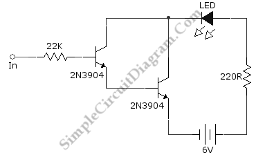
Transistors Q1 and Q2 create a buffer that offers the probe a suitable input impedance. Q3 and Q4 constitute a level detection circuit. When the voltage across the base-emitter junction of Q3 exceeds 0.6 V, the transistor activates, which...
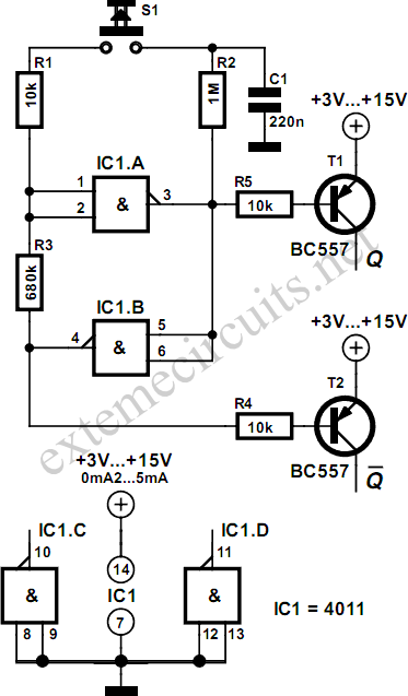
Using just two NAND or inverter gates, it is possible to build a D-type (or toggle) flip-flop with a push-button input. At power-up, the output of gate N2 is at a logical 1, ensuring that transistor T2 is switched...
Ideally, any testing equipment will not draw any current from the device under test. This ideal condition can be approximated by designing a testing device. To achieve the ideal condition where testing equipment does not draw current from the device...
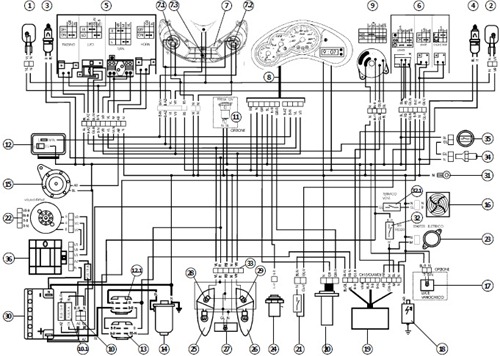
The following presents an electrical schematic for a 1993 VW Passat. Features include vehicle content and electrical wiring schematic. Components consist of console switches, electric windows, ABS control unit, ABS hydraulic unit, engine control module, automatic control unit, fuse/relay...
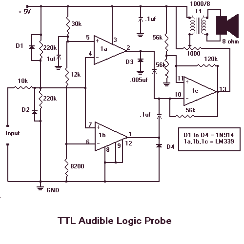
When testing circuits with a logic probe, it is sometimes difficult to watch the LEDs on the probe to determine the logic state. With this probe, the logic states are audible. This probe is designed for TTL circuits only...