
Darlington Transistor Pair Logic Probe

To achieve the ideal condition where testing equipment does not draw current from the device under test (DUT), it is essential to design the testing device with high input impedance. This can be accomplished by utilizing operational amplifiers (op-amps) in a voltage follower configuration, which presents a very high impedance to the DUT.
The circuit can be composed of an op-amp connected in a non-inverting configuration. The output of the op-amp will follow the input voltage while ensuring minimal loading on the DUT. The input terminals of the op-amp should be connected to the DUT, while the output can be routed to a measurement instrument, such as a digital multimeter or an oscilloscope, for voltage readings.
Additionally, the power supply for the op-amp should be carefully selected to match the expected voltage levels of the DUT, ensuring that the op-amp operates within its linear range. Bypass capacitors may be added near the power supply pins of the op-amp to filter out any noise and provide stable operation.
To further minimize the current drawn from the DUT, the testing device can incorporate a high-value resistor in series with the input. This resistor should be large enough to ensure that the current drawn is negligible compared to the operational characteristics of the DUT.
By implementing these design considerations, the testing equipment can effectively approximate the ideal condition of not drawing current from the DUT, allowing for accurate and reliable testing results.Ideally, any testing equipment will not draw any current from the device under test. This ideal condition can be approximated by designing a testing device.. 🔗 External reference
Related Circuits
There are two switches: a memory disable switch and a pulse polarity switch. The memory disable switch is a push-button that resets the memory to a low state when pressed. The pulse polarity switch is a toggle switch that...

The simple transistor tester in Figure 1 allows for the identification of the type of transistor and aids in detecting the emitter, collector, and base of the transistor. The simple transistor tester circuit is designed to facilitate the identification of...
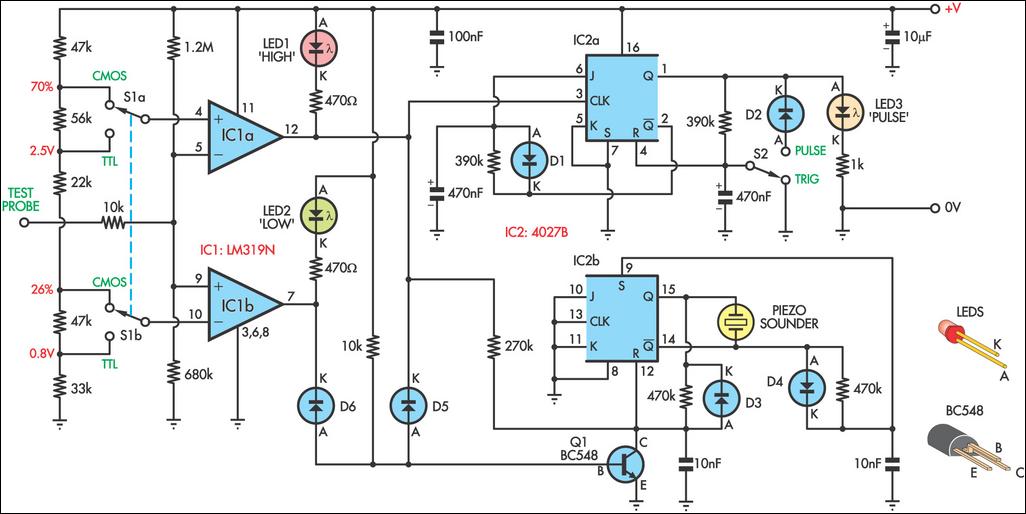
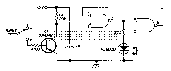
This logic probe can be configured to operate on either TTL or CMOS logic levels using switch S1. A series of resistors connected to switch S1 establishes the threshold levels for a window comparator made up of IC1a and...
An RF probe is a circuit designed for testing equipment that converts high-frequency signals into DC voltage. This conversion facilitates the measurement of RF voltages for testing or adjusting transmitters, receivers, and modulators. The RF probe circuit outlined here...
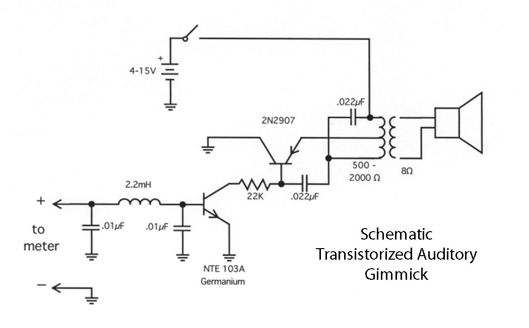
This circuit first appeared in "The Braille Technical Press," edited by Robert W. Gunderson, in 1955. Gunderson, W2JIO, designed this "gimmick" to read transmitter meters. It has appeared many times over a 20-year period, including in commercial aids and...
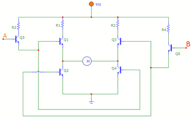
The transistors Q1, Q2, Q3, and Q4 form a bridge circuit. These are typically power transistors designed to handle high current. Transistors Q5 and Q6 drive the bridge. When input A is set high and input B is set...