
Composite pipe circuit

The first configuration, utilizing two transistors of the same type, typically involves a common emitter or common collector arrangement. In this setup, both transistors operate under identical biasing conditions, which allows for consistent electrical characteristics and simplified design. This configuration is often employed in applications requiring signal amplification or switching, as it ensures that the transistors can effectively drive the load with minimal distortion.
The second configuration, which incorporates two different types of transistors, introduces a level of complexity that can be beneficial in certain applications. This approach allows for the combination of different electrical properties and performance characteristics, such as varying gain, frequency response, and input/output impedance. By selecting transistors with complementary characteristics, designers can create circuits that optimize performance for specific tasks, such as analog signal processing or digital logic operations.
Both configurations can be effectively utilized in various electronic applications, including amplifiers, oscillators, and digital circuits, depending on the desired performance and operational requirements. The choice between using identical or different types of transistors will largely depend on the specific application and the performance criteria that need to be met. Proper consideration of the operational parameters and characteristics of each transistor type is essential for achieving the intended functionality and reliability of the circuit.There are two composite pipe constitute ways: one is by the two transistors of the same type, as shown) as shown; the other is composed of two different types of pipe configuration,
Related Circuits
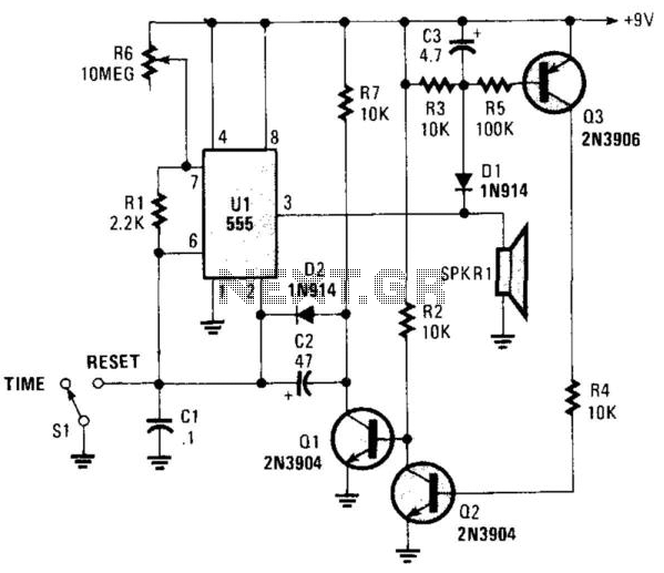
This circuit operates in astable mode and produces a tone at the end of the first period, which can last several minutes. When switch SI is in the time position, transistor Q3 is turned off because pin 3 of...
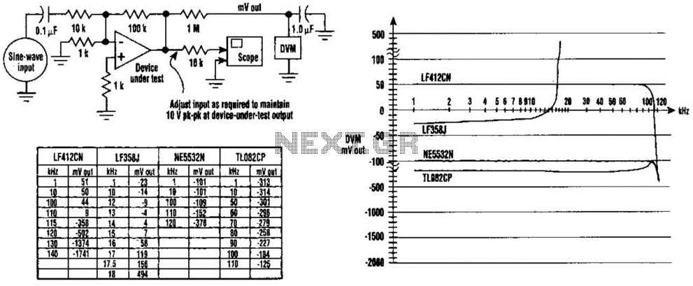
The DC values of op-amp offsets cannot always be assumed to remain constant when delivering AC outputs. No device is perfectly symmetrical in terms of maximum positive slew rate compared to maximum negative slew rate. As a result, there...
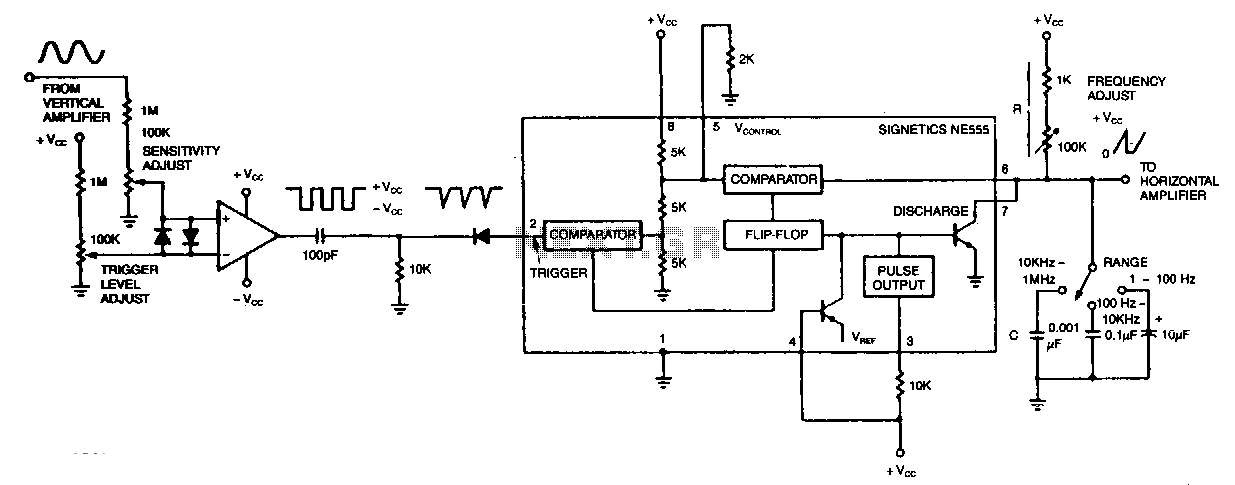
The circuit's input operational amplifier triggers the timer, sets its flip-flop, and cuts off its discharge transistor, allowing capacitor C to charge. When the voltage across the capacitor reaches the timer's control voltage of 0.33 Vee, the flip-flop resets,...
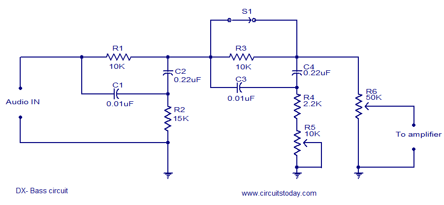
The circuit diagram of a passive DX bass circuit is presented, which is compatible with nearly all audio amplifiers. This design was created by Mr. Emmanuel Chipula from Malawi and submitted for publication. Laboratory tests confirmed satisfactory performance. Credit...
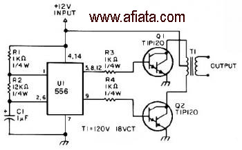
The first section of the 555 timer is configured as an astable oscillator, with R2 and C1 determining the frequency. The output is accessible at pin 5. The second section functions as a phase inverter, with its output available...
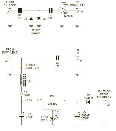
This wideband amplifier circuit is designed using the MAR-6 IC manufactured by Mini Circuits. The MAR-6 VHF-UHF wideband amplifier circuit provides a stable gain of at least 9 dB up to 2 GHz. Since the MAR-6 is designed to...