
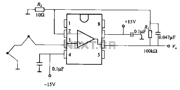
Time-Out Circuit

The described circuit functions as an astable multivibrator, generating a continuous square wave output that produces an audible tone through the speaker. The operational amplifier Ul serves as the core timing component, with its output controlling the state of the transistors Q1, Q2, and Q3. The configuration ensures that the circuit oscillates between two stable states, producing a periodic signal.
In the initial state, when switch SI is engaged, capacitor C1 and C2 are charged, and the voltage across them influences the output of the operational amplifier. The timing period is primarily determined by the values of resistor R6 and the capacitance of C1 and C2, which dictate how quickly the capacitors charge and discharge. The relationship of 1.1 times R6 with the total capacitance creates a predictable timing cycle, allowing for consistent tone generation.
As the cycle progresses, when the output of Ul transitions low, it triggers the turning on of Q3 and Q2, which then alters the state of Q1, effectively disconnecting capacitor C2 from the circuit. This transition allows the circuit to enter the oscillation phase, where the timing is now governed by R7 and C1. The forward biasing of diode D2 permits the oscillation to continue, creating a tone output that is transmitted through SPKR1.
The reset functionality provided by switch S2 allows for the circuit to be restarted, returning it to its initial state. This feature is crucial for applications requiring periodic tone generation, enabling the user to control the start and stop of the oscillation at will. Overall, this astable circuit design is efficient for producing sound signals and can be utilized in various electronic applications, including alarms, timers, and sound-generating devices. This circuit operates in the astable mode and at the end of the first period (up to several minutes), it produces a tone. When SI is placed in the time position, Q3 is cut off because pin 3 of Ul is high and Dl holds Q3 in cutoff. Q2 is off, and Ql is on, which grounds the negative end of D2 and C2. Therefore, CI and C2 are returned to ground. After a time of about 1.1 R6 (Ci + C2), the timer cycle completes and pin 3 Ul goes low. This turns en Q3 and Q2, cuts off Ql, and effectively disconnects C2. Now, the circuit oscillates with a period determined by R7 and CI, because D2 is forward-biased. A tone is then generated and can be heard from SPKR1. Closing S2 resets the circuit.
Related Circuits
The OP07 is a low drift operational amplifier with a maximum voltage drift of 30 µV/°C and a maximum drift of 0.6 mV/V/°C. It features low noise characteristics with a maximum noise level of 0.6 pV/√Hz, offering ultra-stability with...
An RF power amplifier is an electronic amplifier used to convert a low-power radio-frequency signal into a larger signal of significant power, typically for driving the antenna of a transmitter. It is optimized for high efficiency, high output power...
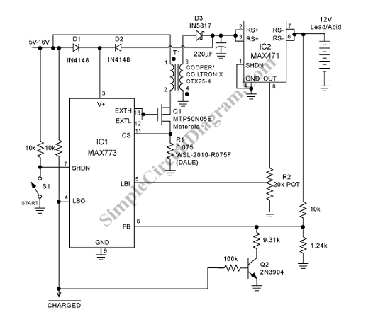
To charge lead-acid batteries, a circuit can be utilized that consists of a current-limited power supply and a flyback converter topology. The circuit designed for charging lead-acid batteries incorporates a current-limited power supply alongside a flyback converter topology to...
Circuit for Grundig 5441 TV. If there are any issues related to this circuit, please provide additional information about the problem for further assistance. By accessing the Fixya site, users acknowledge that they have read and agreed to its...
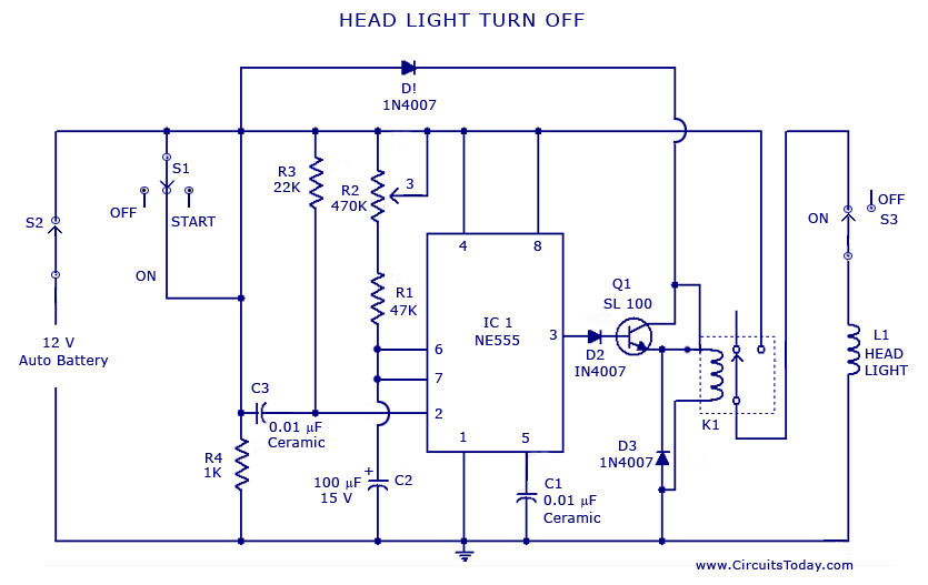
A circuit that can automatically turn off the headlights or lamps of a vehicle after a preset time. This light switching circuit is constructed using a 555 timer integrated circuit (IC). The described circuit utilizes the 555 timer IC in...
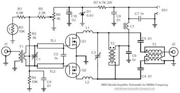
The design of this amplifier aims to enhance the reproduction of complex music and voice. While high electrical properties are emphasized, the primary objective is to achieve superior sound quality, vivid imaging, and exceptional spatial clarity. Although the average...