
Oscilloscope triggered sweep circuit

The described circuit utilizes an operational amplifier (op-amp) as a comparator, which plays a critical role in controlling the timing sequence. The op-amp compares the voltage across capacitor C with a reference voltage equivalent to 0.33 times the supply voltage (Vee). When the input voltage from the op-amp exceeds this threshold, it triggers the timer circuit, which is typically configured using a monostable or astable multivibrator configuration.
The timer's output is connected to a flip-flop, which serves to maintain the state of the circuit during the timing interval. When the flip-flop is set, it disables the discharge transistor, allowing capacitor C to charge through a designated charging path. The charging time is determined by the RC time constant, where R is the resistance in series with the capacitor, and C is the capacitance value.
Once the voltage across the capacitor reaches the specified control voltage, the flip-flop resets. This action enables the discharge transistor, which creates a path for the capacitor to discharge rapidly. The discharge path is crucial for resetting the circuit to its initial state, allowing for subsequent cycles of operation.
To enhance the linearity of the timing behavior, a constant-current source can be introduced in place of the variable resistor R used for frequency adjustment. This modification ensures that the charging current remains stable, resulting in a more predictable and linear voltage rise across the capacitor. Such an improvement is particularly beneficial in applications requiring precise timing intervals and consistent performance across varying conditions.
Overall, this circuit design effectively demonstrates the interplay between analog components, providing a reliable method for timing applications while allowing for adjustments to optimize performance characteristics.The circuit"s input op amp triggers the timer, sets its flip-flop and cuts off its discharge transistor so that capacitor C can charge. When capacitor voltage reaches the timer"s control voltage of 0.33 Vee. the flip-flop resets and the transistor conducts, discharging the capacitor.
Greater linearity can be achieved by substituting a constant-current source for frequency adjust resistor R.
Related Circuits
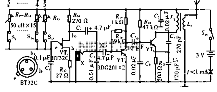
The circuit operates with VT3 and associated components arranged as a common-base capacitance feedback oscillation circuit. The oscillation frequency is set by capacitors C8, C9, and inductor L1. VT2 serves as a voltage amplification stage that reinjects the audio...
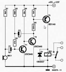
This sound-activated switch allows for control through sound, which can be beneficial not only in robotics but also in home automation applications. The sound-activated switch operates by detecting specific sound frequencies or patterns, typically using a microphone or a sound...
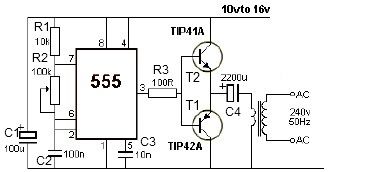
This 12V power inverter circuit can be utilized to power small devices that require 240 volts. It is particularly advantageous for operating 240-volt appliances using a 12-volt car battery. Unlike typical feedback oscillator inverters, this design employs a 555...
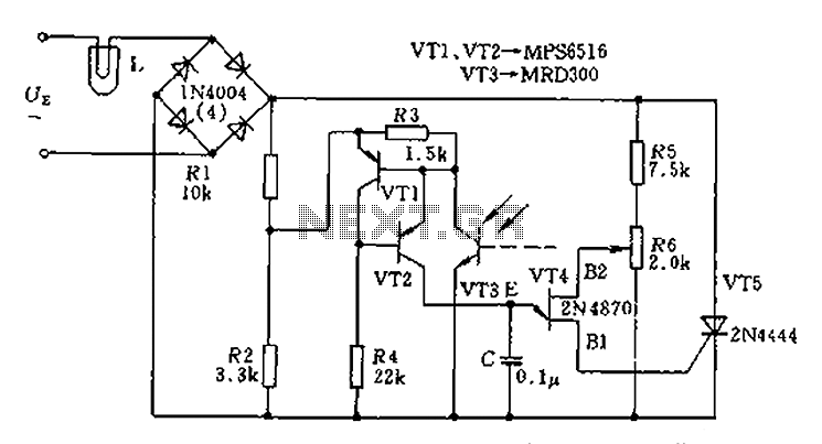
The circuit is designed to stabilize the brightness of lamp L using a thyristor-based AC automatic voltage regulator. The thyristor T5 is connected diagonally across the bridge circuit. The trigger pulses are generated by components VT1, VT2, and VT3,...
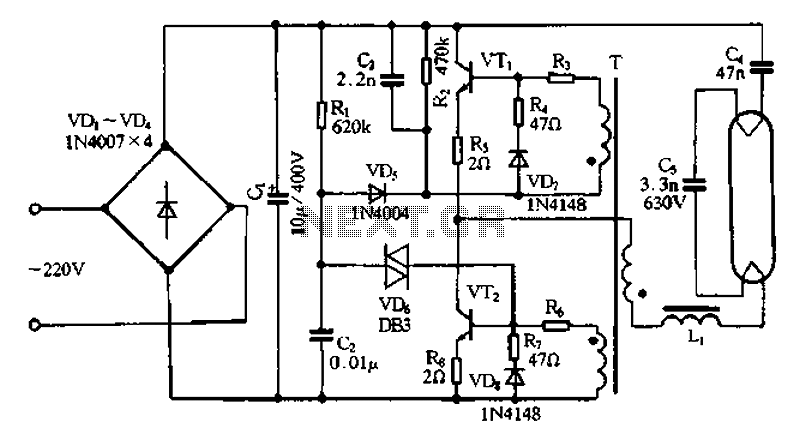
Bridge rectifier circuit in the electronic ballast application circuit The bridge rectifier circuit is a crucial component in electronic ballast applications, primarily utilized for converting alternating current (AC) to direct current (DC). This conversion is essential for powering various electronic...
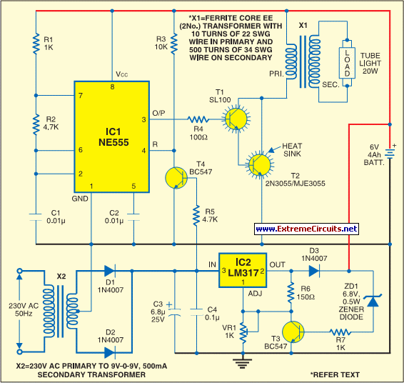
The circuit consists of inverter and charger sections. The inverter section utilizes the NE555 timer, while the charger section is based on the LM317 adjustable regulator. In the inverter section, the NE555 is configured as an astable multivibrator, generating...