
Differential A/D Converter circuit CA3110

The BiMOS CA3140 operational amplifier is a versatile component characterized by its high bandwidth and rapid response to signal changes. This op amp is particularly effective in applications requiring precise signal conditioning and amplification. Its ability to function near the negative supply rail enhances its utility in various circuit designs, allowing for greater flexibility in system configurations.
In scenarios where the input voltage may exceed the supply voltage VDD, it is crucial to protect the op amp from potential damage caused by overvoltage conditions. The implementation of a clamp diode serves as an effective protective measure. By connecting a diode from pin 8 of the CA3140 to the VDD supply, any excess voltage can be safely redirected, preventing the op amp from being subjected to harmful levels.
The schematic for this configuration should include the CA3140 op amp, clearly labeling the input and output terminals, as well as the power supply connections. The clamp diode should be represented with its anode connected to pin 8 and the cathode connected to the VDD. This arrangement ensures that the op amp operates within its specified voltage limits, thereby enhancing reliability and performance in high-frequency applications. Proper grounding and decoupling capacitors should also be included in the design to minimize noise and improve stability.By using an op amp BiMOS CA3140 provides good orientation skills for high bandwidth signal input, and can quickly adjust the energy output at its terminal CA33IO WINE. The CA3140 can also lead to near the negative supply rail. If the sequencing system power or voltage input is known to cause the op amp to drive above the supply VDD, a clamp diode can be added from pin 8 of op amp to power supply VDD.
Related Circuits

TMP01 is a temperature sensor that features a programmable temperature controller, an integrated reference voltage source, a current source, a voltage comparator, and an amplifier circuit. The internal circuit function block diagram and basic application circuit are provided. The key...
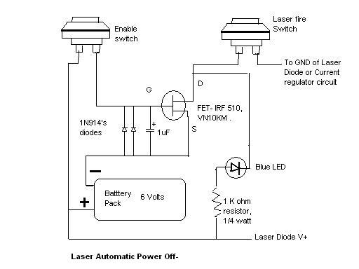
Here is the automatic laser power-off circuit schematic. This circuit features a visible power indication. In this case, the ground is connected on one side. The automatic laser power-off circuit is designed to enhance safety and efficiency in laser applications...

This power inverter circuit provides a stable square wave output voltage. The frequency of operation is set by a potentiometer and is typically adjusted to 60 Hz. Various off-the-shelf transformers can be utilized, or custom-wound transformers can be created...
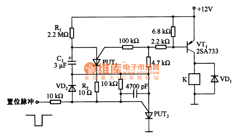
Figure 1 illustrates an enhanced trigger timing circuit that utilizes two Programmable Unijunction Transistors (PUTs). When a set signal is applied, the circuit is activated, causing transistor VT1 to enter the conduction state and energizing relay K. This action...

This electronic RF detector project is constructed using common transistors and a few standard electronic components. The RF detector is capable of responding to RF signals below the standard broadcast band and extending to over 500 MHz, providing both...
A pulse booster circuit is utilized to increase the pulse amplitude. The structure illustrated in figure (a) of the circuit can output a pulse amplitude that is twice that of the input. Figure (b) of the circuit can achieve...