
Fan automatic control circuit

This bistable circuit operates as a memory element, maintaining its state until triggered to change by external control signals. The control mechanism relies on the high and low levels of the output, which govern the state of the circuit. The full-wave rectification process ensures that the input AC voltage is converted into a stable DC voltage, crucial for the reliable operation of the circuit.
The role of the ZD and ZD2 components as secondary regulators is to maintain a consistent output voltage despite variations in input voltage or load conditions. This regulation is essential for preventing damage to sensitive components within the circuit. The electronic filtering provided by VT1 helps to smooth out any ripples in the DC output, further ensuring stable operation.
The capacitors C1, C3, and C6 are integral in stabilizing the voltage across critical points in the circuit. Their ability to absorb and release energy mitigates voltage spikes that could otherwise disrupt the operation of the integrated circuit (IC) and the flip-flop outputs. The behavior of transistors VT1, VT2, VT4, and VT3 illustrates the importance of biasing in transistor operation, where the base-emitter voltage determines whether the transistor is in an on or off state.
The charging process of capacitors C2, C4, and C6 through resistors R4 and R8 is a critical aspect of timing within the circuit. The time constant, determined by the resistance and capacitance values, dictates how quickly these capacitors charge to the supply voltage. This charging period is essential for the proper timing of the circuit's response to control signals.
In summary, this bistable circuit is a well-designed system that utilizes various electronic components to achieve stable operation, effective voltage regulation, and reliable control over connected loads such as lights and motors. The interplay between capacitors, resistors, transistors, and thyristors illustrates fundamental principles of electronics, making this circuit a valuable example of practical circuit design. Box circuit) bistable circuit, each bistable circuit is a single bond by the control output high and low level. When the circuit instant access electricity, electricity through R13, cl, buck, VD, VD2 full-wave rectification, ZD, ZDz secondary regulator, then by VTs electronic filtering, got 8.V DC voltage. Because the capacitance C., C3, C, not the voltage across the energy mutation, so the IC, the input 1,5,11 pin is low, the corresponding inverter output terminal 6, 10 feet high, so each the output of flip-flop circuit terminal 4, 8, 12 feet low.
Thus, the transistor VT, VT2, VT4 base is extremely high, VT VT,, VT4 off, the VT3 base is extremely low, VT3 conduction. Because VT4 close, so VT3 no collector current, therefore, the thyristor vs, VS2, VS3 no trigger current is turned off, lights L is not lit, the motor M does not turn.
And the same time the capacitor C2, C4, C6 via a resistor feet, R4, Rg charged within about 0.1 8 can be charged to the supply voltage 8.5 V.
Related Circuits

RTD sensors are measured using a precision 24-bit analog-to-digital converter (A/D) that includes a built-in programmable gain amplifier. The connections for 2-wire, 3-wire, and 4-wire RTDs are illustrated. This setup facilitates the connection and measurement of RTDs with amplifiers and...

Using a battery, a phototransistor, and a visible-light LED, this simple circuit functions as a "go/no go" tester for infrared remote control devices. The illumination of the LED indicates that the phototransistor is being modulated by infrared energy. This circuit...

The VE1 preamplifier utilizes a low muscle, low resistance double triode 6N6 configuration, with separate halves for the left and right audio channels. The design operates within the CPI framework. It promotes the use of high-level VE2 household low...
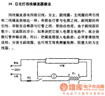
The four-wire ballast connection of a fluorescent lamp consists of four lead wires, which include main and auxiliary coils. The connection of the two lead wires in the main coil is similar to that of a second-line ballast; both...

A code practice oscillator was built some time ago, and there is a vague recollection of the project. It featured a straight key that plugged directly into the key jack. Upon opening the device, a circuit board populated with...

The current generated flows through clips placed on the earlobes. The output current is adjustable from 80 to 600 microamperes, following the recent launch in Europe. The described device utilizes a current generation mechanism that delivers a controlled microcurrent through...