
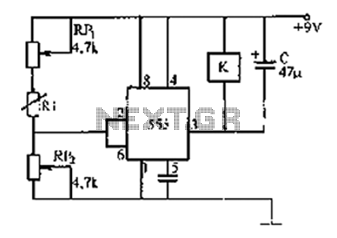
frequency conversion circuit composed of NE555

The circuit utilizes the NE555 timer IC in astable mode to generate a continuous square wave output. The frequency of oscillation is primarily determined by external components, including resistors and capacitors connected to the NE555. In this configuration, VT2 acts as a control element, modulating the discharge cycle of capacitor C2.
When the output at pin 3 of the NE555 is low, VT1 is turned off, which allows VT2 to conduct. The current Ic2 flowing through VT2 is influenced by the output voltage from amplifier Al, which serves to stabilize the circuit's operation. The formula for discharge time T1 indicates that the time constant is directly proportional to the capacitance of C2 and the voltage U2, while inversely related to the current Ic2. This relationship is critical for determining the frequency of oscillation and ensuring the desired performance of the circuit.
The stable voltage Uz across diode VD1 plays a significant role in maintaining the circuit's reliability, providing a reference point for the voltage levels involved in the timing cycle. The interplay between these components allows for precise control over the timing characteristics of the NE555, facilitating applications in timer circuits, pulse generation, and frequency modulation. Proper selection of the values for C2, the resistors in the timing network, and the characteristics of VT2 and Al is essential for achieving the desired oscillation frequency and waveforms.In the circuit, NE555`s oscillation frequency is controlled by the VT2, and during its pin 3 in the low output waveform (output waveform of the T1 period), as VTI stops, VT2 is conduction with current Ic2 flowing, and the size is controlled by the output voltage of Al. C2 discharge time T1 = C2U2 / (2Ic2), in the formula, Uz is the stable voltage of VD1. NE5.. 🔗 External reference
Related Circuits
This gated 1-kHz oscillator provides a press-to-turn-on functionality, with waveforms available at the output of pin 3 and across capacitor CI. The gated 1-kHz oscillator circuit is designed to produce a square wave output that can be activated by a...
Men often appreciate the convenience of television remote controls, which can sometimes frustrate their female partners. They tend to switch channels frequently, wanting to ensure they do not miss anything while a specific program is on. With the remote...

This circuit represents a waveform generator, which is highly beneficial for electronic experiments and design. It primarily generates sine wave oscillations, but the circuit can be modified to produce triangle or square wave functions. The circuit is based on...
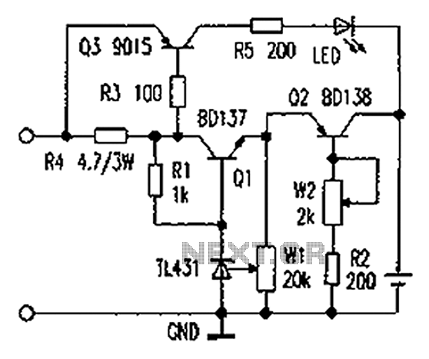
As illustrated in the figure, the lithium battery charging control board employs a constant current charging mechanism. The components Q1, R1, W1, and TL431 form a precision adjustable voltage regulator circuit. The components Q2, W2, and R2 create an...
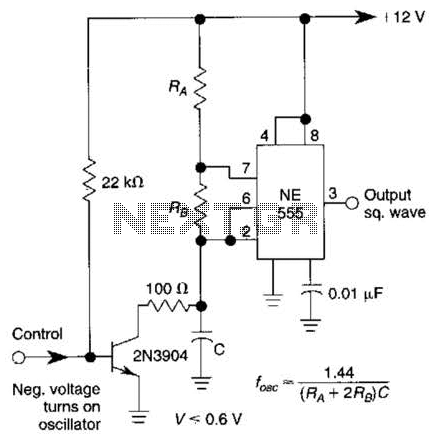
The 555 timer integrates both analog and digital functions within a scaled integrated device. Typically manufactured using a bipolar process, it is designated as the 555 timer, while the CMOS version is referred to as the 7555. In addition...
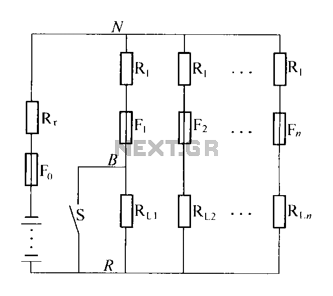
The circuit diagram illustrates a high-impedance distribution system characterized by low resistivity distribution. A notable feature is the series resistance of the shunt load current limiting resistor R1, typically valued at five to ten times the internal resistance of...