
Heath SB-200 keying circuit
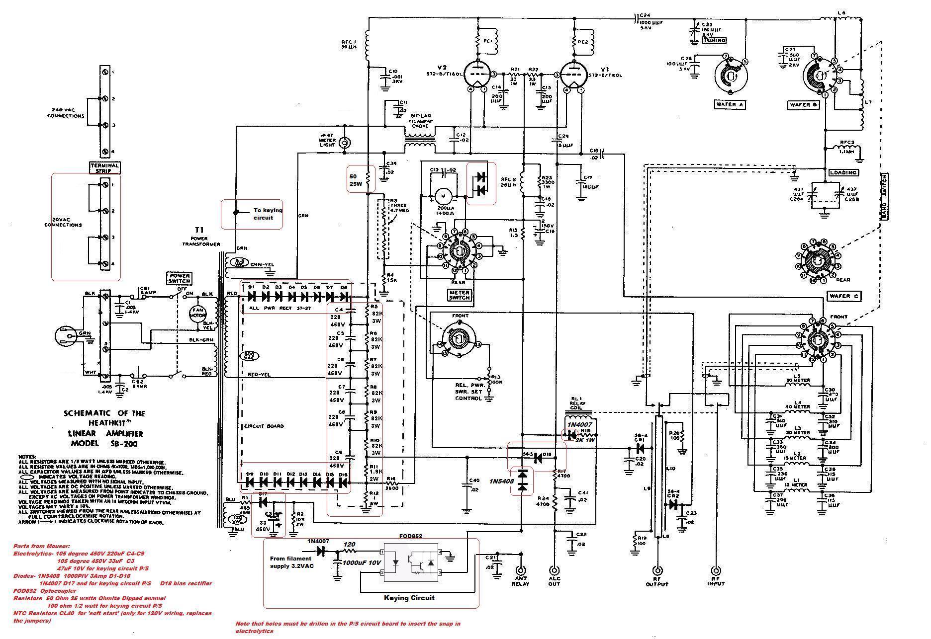
The described circuit is designed to function as a keying mechanism for RF amplifiers, specifically tailored for the SB-200 model. The keying circuit allows for the controlled operation of the amplifier, ensuring that it engages and disengages efficiently during transmission and reception modes.
The schematic typically includes essential components such as transistors, resistors, capacitors, and diodes, which work together to create a reliable switching mechanism. The transistors are often used as switches to control the flow of power to the amplifier, while resistors and capacitors help to manage the timing and stability of the circuit.
In a standard configuration, a small signal from a transmitter or keying device is fed into the base of a transistor, which then allows a larger current to flow from the power supply to the amplifier, effectively turning it on. Conversely, when the signal is removed, the transistor cuts off the current, turning off the amplifier. This method not only provides an economical solution but also ensures that the amplifier operates safely and effectively without the need for expensive commercial keying circuits.
In summary, this modified keying circuit is a practical and efficient solution for users seeking to enhance their SB-200 amplifier's performance while minimizing costs. The schematic serves as a valuable reference for those looking to implement similar modifications in their equipment.For those who may want to try a cheaper alternative to the commercially available keying circuits. Works well in my SB-200. Here is a schematic of my modified SB-200.. 🔗 External reference
Related Circuits
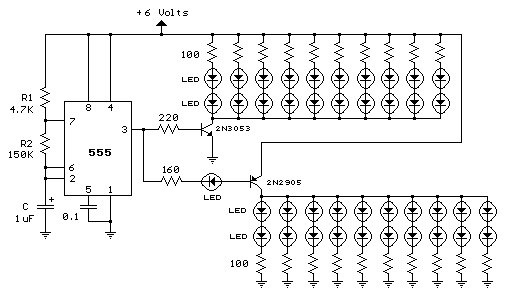
This LED series will blink alternately. The operation is determined by the NE555 integrated circuit, with transistors used to reinforce each section (20 upper, 20 lower) for optimal performance. The 555 circuit described below functions as a flashing bicycle...
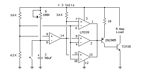
In this circuit, an LM339 quad voltage comparator is used to generate a time delay and control a high current output at low voltage. Approximately 5 amps of current can be obtained using a couple of fresh alkaline D...
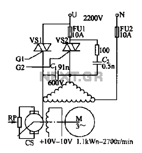
AC voltage is rectified by a bridge (VD1-VD4). A resistor (R1) limits the buck, while diode (VD5) provides clipping. A trapezoidal wave is generated as the trigger circuit for DC voltage and synchronization. When the base of transistor (VT1)...
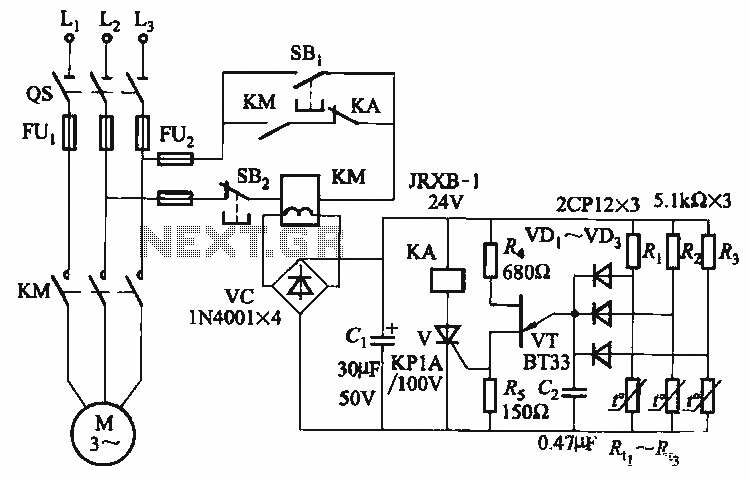
The thyristor control circuit includes a bridge circuit designed to regulate the temperature in the contactor coil KM, along with a secondary winding that functions as a power protection device. It comprises a thermistor (R:., Rt3) and a resistor...
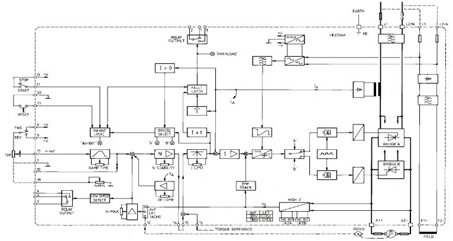
This figure represents the 4Q2 DC Motor Speed Controller Circuit Block Diagram, designed for comprehensive control of conventional shunt-wound and permanent magnet motors with a capacity of up to 75 kW, as specified in the datasheet. This type of...
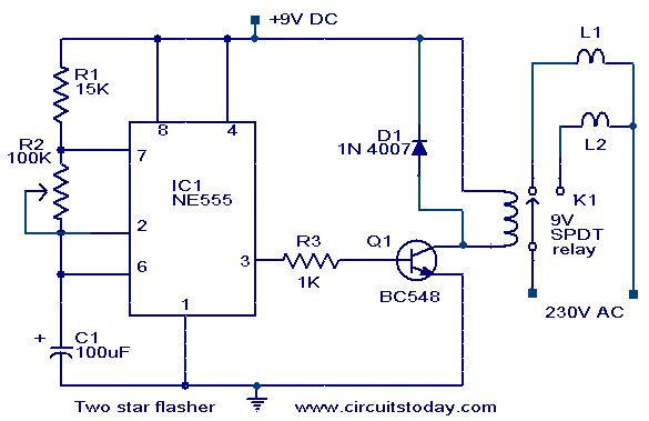
A circuit designed to alternately flash two Christmas stars is presented. The NE555 integrated circuit (IC1) is configured as an astable multivibrator. When IC1 outputs a positive pulse, transistor Q1 becomes conductive, activating relay K1. Consequently, lamp L2, connected...
Warning: include(partials/cookie-banner.php): Failed to open stream: Permission denied in /var/www/html/nextgr/view-circuit.php on line 713
Warning: include(): Failed opening 'partials/cookie-banner.php' for inclusion (include_path='.:/usr/share/php') in /var/www/html/nextgr/view-circuit.php on line 713