
High voltage (120V), converting familiar fast (120V Shu us) power MOSFET Amplifier circuit
, converting familiar fast (120V Shu us) power MOSFET Amplifier")
The described south circuit is a complex assembly of transistors designed for efficient signal processing and amplification. The NPN transistor (T1) acts as a dynamic garbage collector, filtering unwanted noise from the input signal. This is essential in maintaining signal integrity, particularly in environments with significant electromagnetic interference.
The PNP differential amplifier (T2, T3) operates as a double differential circuit, which enhances the circuit's ability to reject common-mode signals while amplifying the differential signal. This configuration is particularly beneficial in applications requiring high precision and stability, as it ensures that any noise common to both inputs is minimized.
The voltage amplification stage, utilizing photo transistors (T4, T5), is critical in determining the output amplitude. These transistors are designed to handle high bias voltages, which allows for better performance in terms of linearity and dynamic range. The absence of a phase compensation capacitor in the collector-base junction of T1 and T2 can lead to potential issues with conversion rates, particularly under varying load conditions.
The bias circuit serves a dual purpose: it stabilizes the output stage by eliminating unwanted voltage at the base and ensures that the circuit operates within a defined quiet area. This is crucial for maintaining performance, especially when the output stage is subjected to no-load conditions, where excessive current might otherwise flow.
Transistor T3 plays a vital role in protecting the output stage from short-circuit conditions by limiting the maximum drain current. This is a critical safety feature, ensuring that the circuit can withstand fault conditions without sustaining damage.
The voltage division described indicates a mechanism for controlling the activation of the transistors based on load conditions. When the voltage across the load reaches 0.5V, it triggers the transistor to turn on, thereby regulating the current flow and ensuring that the circuit operates within established domestic standards. This feature is essential for maintaining compliance with safety regulations and ensuring reliable operation in practical applications.
Overall, the south circuit is a sophisticated design that effectively combines various transistor configurations to achieve high-performance signal processing, amplification, and protection against faults, making it suitable for a wide range of electronic applications.The south circuit composed of four parts, the order of descent {NPN transistor whole dynamic garbage dog device (Tfl ", Tr song and PNP transistor differential amplifier Phi (TrS, Tt.4) double differential circuit, two balanced amplifier C output opposite phase), and the drive voltage amplification photo (Trs. Tri) port voltage amplifier stage is an important component determines the output amplitude and conversion Qu sneeze should be possible to work under a large bias Tong.
Because Tr ,, TT8 collector base valve without a vote plus phase compensation capacitor, it is possible to reduce the conversion rate of decline. Trr bias circuit is used to eliminate the base voltage of the output stage q quiet area with yR. You can not pay the entire signal current output stage (or no-load electric reservoirs); r_, Tr- is used to limit the maximum drain current of the output stage circuit, play load short-circuit protection.
Chu 1. , Set i. To reveal "the voltage across the 'I mouth lIi ,, x chu means D) dividing the voltage as Garnet had 0.5y, the transistor will be turned on by the suction 5fT'_l income TrIo base electric comb, so that electrical limit village gangrene in certain domestic norm.
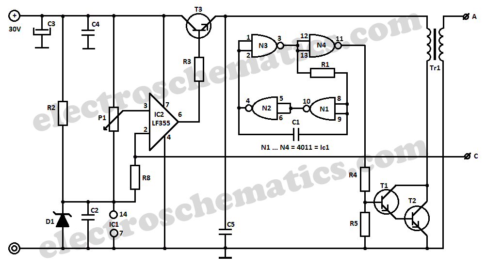
Related Circuits
This DIY 12V to 220V DC to AC converter utilizes a CMOS 4047 as its main component, effectively transforming 12V DC into 220V AC. The circuit design of this DC to AC converter primarily revolves around the CMOS 4047 integrated...
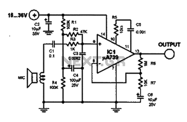
This microphone preamplifier utilizes the low-noise integrated circuit (IC) uA739. It serves as a practical example of designing an effective preamplifier for dynamic microphones. The IC contains two identical integrated preamplifier circuits, with the second preamp functioning in the...
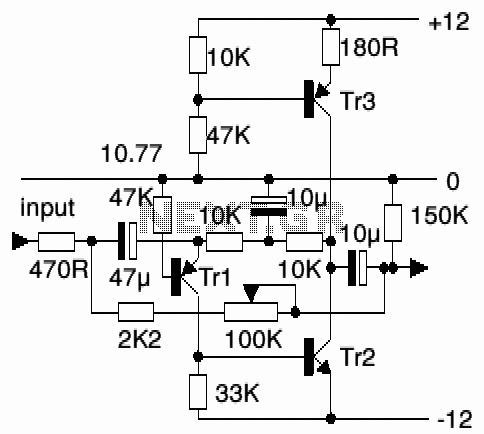
Electronics Circuits Reference Archive Audio preamplifier circuits. There are thousands of preamplifier circuits. Here are three that are somewhat different and have garnered interest. Intercom preamp: A very convenient way of making an intercom system. Audio preamplifiers are essential components...
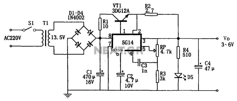
As shown in the figures, this is a practical adjustable power supply. It utilizes an integrated voltage regulator (5G14) in conjunction with a 3DG12A transistor for current spreading, providing an output voltage range of 3 to 6V. The rated...
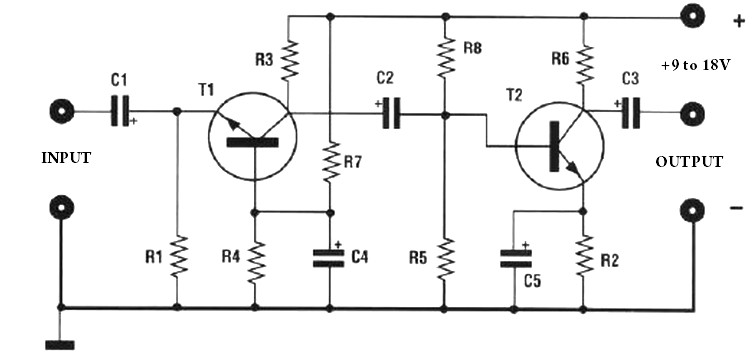
The amplification of this preamplifier is very high. To reduce the amplification, a trimmer resistor R3 in series with a value of 100 ohms should be used. The system can be powered by a voltage ranging from 9 to...
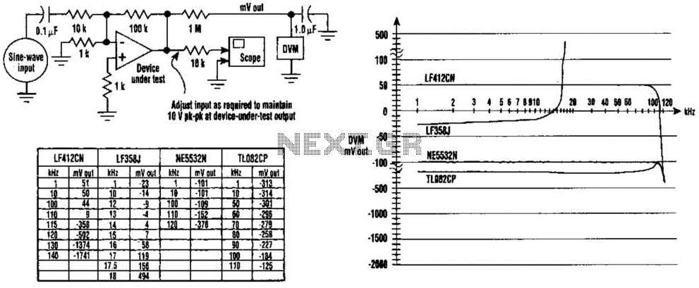
The DC values of op-amp offsets cannot always be assumed to remain constant when delivering AC outputs. No device is perfectly symmetrical in terms of maximum positive slew rate compared to maximum negative slew rate. As a result, there...