
IFA Antenna matching for CC2500

The IFA (Inverted-F Antenna) designed in Altium is intended for operation at 2.4 GHz, making it suitable for applications such as wireless communication and IoT devices. The design process involves careful consideration of the PCB thickness, as this parameter significantly influences the antenna's performance, including gain, bandwidth, and efficiency. The choice to use a two-layer PCB while limiting the antenna implementation to the top layer is strategic, as it can reduce complexity and improve the antenna's performance by minimizing substrate losses.
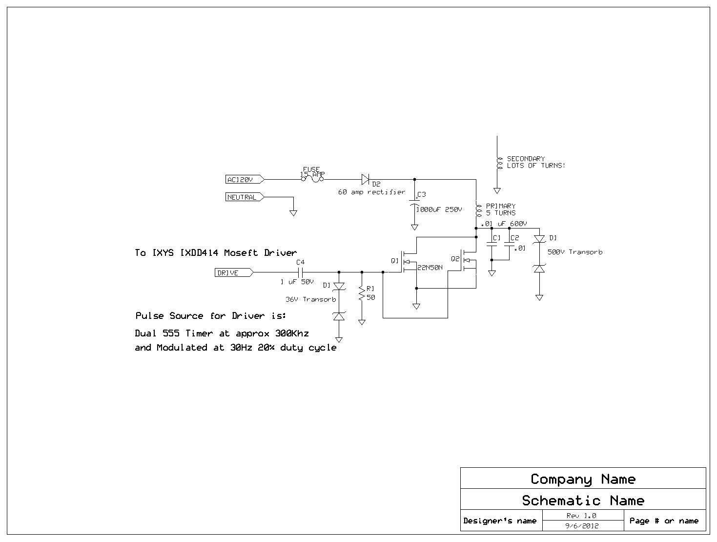
The implementation of a balun circuit derived from the CC2500EM Reference Design is essential for transforming the unbalanced feed from the transmission line to the balanced load of the antenna. This transformation helps in maintaining the desired impedance match, which is critical for efficient power transfer and minimizing signal reflections.
Considering the possibility of using a 50 Ohm transmission line is prudent, as it matches the standard impedance used in RF applications, ensuring compatibility with most RF components and reducing potential signal loss. The suggestion to incorporate a pi-network for impedance matching is also noteworthy. This network typically consists of two capacitors and one resistor, configured in a manner that allows for fine-tuning of the impedance seen by the antenna. The pi-network can be especially useful in scenarios where the antenna may become detuned due to environmental factors or physical obstructions.
The recommendation to add the pi-network after C2134 serves as a safeguard against mismatch, ensuring that the system maintains optimal performance under varying conditions. If the antenna's impedance deviates from the expected 50 Ohm, the pi-network can compensate for this mismatch, allowing for a more robust and reliable communication link.
Overall, the design approach reflects a solid understanding of RF principles and the practical considerations necessary for successful antenna implementation. The careful selection of components, along with the strategic use of network configurations, will contribute to the overall efficacy of the antenna system.I`ve designed IFA antenna in Altium as described in DN007 and created a balun circuit from the schematic design of CC2500EM Reference Design (swrr016a). I`m very new to RF designs, as I could understand from application notes and forum posts; this design shall work with the right thickness of PCB.
My PCB will be a 2 layer PCB and I`m planning to u se only the top layer to be the PCB antenna, for maximum range shall I use layer stacking (use both of the PCB layers ) and shall I use a 50 Ohm transmission line on the connection of antenna after connected to balun circuit DN007 antenna is an excellent choice for 2. 4 GHz operation. Just copy the antenna in the reference design onto the top layer. Some of the new antenna reference design which have been released use two layer to increase the bandwidth and to achieve a slight higher efficiency.
DN007 has a wide bandwidth and has already high efficiency so there is no need here to use both pcb layers. Can be a good idea to insert a pi-network between on the 50 feedline forantenna matching purposes. This will guarantee that the antenna mismatchingcan be kept to a minimum. First of all thank you for your fast response. I`ll have one more question regarding to the issue, by "pi-network" did you mean the balun circuit design below And do you think that the schematic design below seems like it`ll work well A pi-network could be added after C2134 just as a safety measure if the antenna would be detuned / mismatched by its physical surroundings.
DN007 has a good match to 50 ohm so more than likely a 0 ohm resistor is sufficient in the pi-network. If the antenna is detuned then the mismatch can be corrected by the pi-network. All content and materials on this site are provided "as is". TI and its respective suppliers and providers of content make no representations about the suitability of these materials for any purpose and disclaim all warranties and conditions with regard to these materials, including but not limited to all implied warranties and conditions of merchantability, fitness for a particular purpose, title and non-infringement of any third party intellectual property right.
TI and its respective suppliers and providers of content make no representations about the suitability of these materials for any purpose and disclaim all warranties and conditions with respect to these materials. No license, either express or implied, by estoppel or otherwise, is granted by TI. Use of the information on this site may require a license from a third party, or a license from TI. Content on this site may contain or be subject to specific guidelines or limitations on use. All postings and use of the content on this site are subject to the Terms of Use of the site; third parties using this content agree to abide by any limitations or guidelines and to comply with the Terms of Use of this site.
TI, its suppliers and providers of content reserve the right to make corrections, deletions, modifications, enhancements, improvements and other changes to the content and materials, its products, programs and services at any time or to move or discontinue any content, products, programs, or services without notice. 🔗 External reference
Related Circuits
The Tab antenna is a folded monopole that you miniaturize by forming it into an inverted L with a downward bend at the end. You can solder it perpendicular to a pc board or build it as part of...
Loop Antennas are considered to be small when their diameter drops below about 1/10 of the wavelength they are intended to be used at. In this case, the term "Tiny" is used because the antenna's diameter is about 1/30,000...
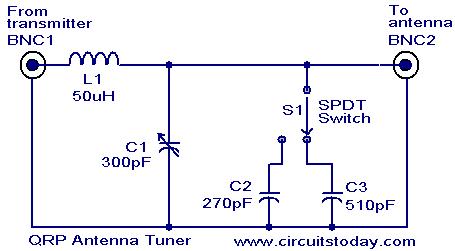
Low power (3 to 30 MHz) transmitters constructed by amateur radio operators are commonly referred to as QRP transmitters. A well-tuned antenna is essential for these transmitters; if the impedance is not properly matched, the output will be minimal...
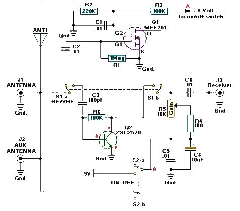
A simple and efficient active antenna electronic project can be designed using this electronic schematic circuit based on transistors. This active antenna project is effective for a wide range of RF frequencies, covering three RF bands: HF, VHF, and...
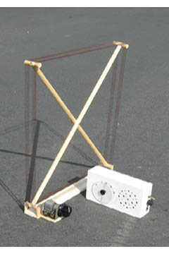
A Tesla Coil can be understood as a high-power radio frequency transmitter with an inefficient antenna. The secondary coil functions as a significantly shortened quarter-wave antenna. The Tesla Coil is an electrical resonant transformer circuit that is designed to produce...
A loop antenna can greatly improve medium wave reception. Loop antennas are directional and receive signals along the plane of the windings. The directional quality improves signal to noise ratio of the desired signal while rejecting signals perpendicular to...