
Inductor saturation tester alternative route to dump the excess energy
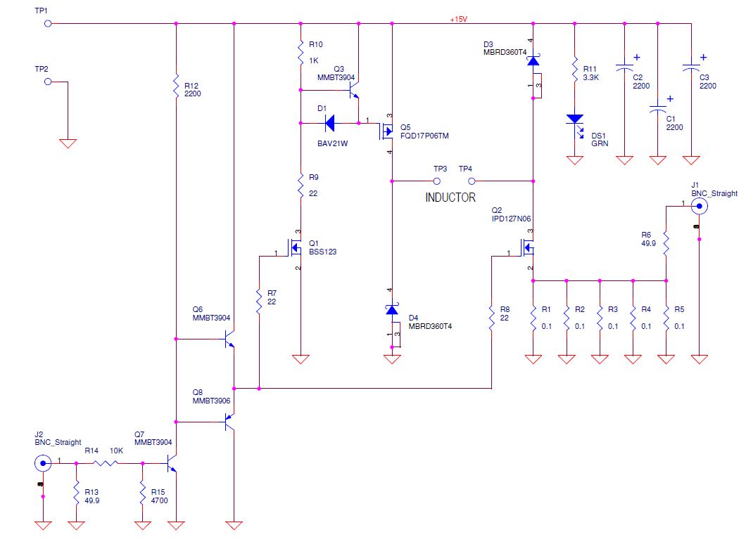
The circuit described involves an inductor charging and discharging mechanism, where diodes play a crucial role in preventing back charging of the inductor while managing power dissipation. The use of a resistor in parallel with one of the diodes is proposed to mitigate issues related to charging time, especially when operating at lower pulse frequencies. The design aims to leverage a PWM generator for signal modulation, which simplifies the control mechanism while allowing for effective duty cycle adjustments through a comparator.
In practical applications, monitoring the current through the inductor is essential to optimize performance and prevent damage to the FETs. Implementing a feedback mechanism to halt FET operation when negative current is detected could enhance efficiency, although it may introduce complexity into the design.
The oscilloscope traces provide valuable insights into the operation of the circuit, showcasing the inductor's behavior during charging and discharging phases. The sharp transitions observed in the waveforms are indicative of the rapid changes in current as the MOSFET switches states. The energy dissipation characteristics, particularly during the ringing phase, are critical for understanding the overall efficiency of the circuit.
This design approach emphasizes the importance of careful component selection and configuration to achieve the desired performance metrics while maintaining simplicity in the circuit layout. The choice of a 555 timer for PWM generation and the LM311 for signal comparison reflects a focus on utilizing readily available components to facilitate ease of construction and troubleshooting.
Overall, the circuit demonstrates a balance between complexity and functionality, aiming to create an effective energy management system while fostering an educational environment for further exploration and development in electronic circuit design.Yes, it does charge the inductor again. Diodes are a good that they will not charge the inductor back but of course dissipate fair amount of instantaneous power due to the forward voltage drop. One way would be to monitor the current and stop driving those fets when the current turns negative, but I guess that is quite complex solution.
I think that a suitable resistor in parallel of the left diode will solve that charging problem, provided that you are not in a hurry to charge the capacitor, i. e. the pulse frequency is low enough, so that there is enough time to charge the capacitor before the next pulse.
To be honest, the reason I started this thread was to start learning and trying to build much simpler one compared to Janne`s nicely built, and the idea of dissipating the excess energy from the inductor popped out while learning it. In my version, the plan is to build a standalone unit with the signal will be supplied by using a much simpler pwm generator like using a 555 for generating the triangle wave and a comparator maybe like LM311 with a pot for duty cycle adjustment in order to get a really small pulse at low frequency.
This should be workable right Those scope shots are really nice, and if its not too troublesome, please shorten the pulse maybe like 10us to get close to the "knee" without the signal shooting up too high to show the complete cycle nicely in the scope screen. And from your traces, it looks like the inductor decaying speed was so fast. Also how is the discharge cycle when the inductor was releasing the energy Again, if you had a chance, please do trace the TP4 point, curious to see how the voltage jumps at the point during the decay period.
Off topic, your TCP202 decaying red trace is slower with a slope compared to the black inductor trace which is straight vertical, why is that The probe`s limitation In this first picture I have `zoomed out` to show the more of the cycle. The upper trace is the output from J1. The sharp edge is caused when the MOSFET Q2 is turned off, it is no longer possible to measure the inductor current.
The current draw from the 10V power supply from this test was 0. 058A, which is 0. 58W and this includes all the power consumption in the gate drive circuitry. In this first picture I have `zoomed out` to show the more of the cycle. The upper trace is the output from J1. The sharp edge is caused when the MOSFET Q2 is turned off, it is no longer possible to measure the inductor current. During the decaying period, once the inductor`s voltage (minus diodes drop out) is equal to power supply rail, the inductor will self dissipate the rest of it`s own excess energy through the ringing as observed at the scope shot, am I correct Just curious and purely academical here, curious in ball park number on how much percentage of the energy left in percentage of total only at that ringing period The current draw from the 10V power supply from this test was 0.
058A, which is 0. 58W and this includes all the power consumption in the gate drive circuitry. I`m aware of the energy required to charge those big caps when the circuit was turned on for the 1st time, but lets ignore this initial state, from this result that this circuit draws only 58 ma at 10 volt is pretty low isn`t it This is valuable info, so I don`t need a beefy power supply. The reason is, say for an inductor with high inductance and high current saturation, this will have a really slow di/dt or shallow loong trace, so the easier part is to cr
🔗 External reference
Related Circuits
The design is based on concepts from K8CU and AG6K, but the circuit has been simplified and uses different components. The mechanical encapsulation has also been modified. LTspice was utilized to verify the tester prior to construction. The schematic...

A thorough examination of the Kapanadze video reveals that the vertical coil is wound with copper tape, forming a capacitor that captures environmental particles with the assistance of high voltage. Experiments indicate that it charges easily with minimal power...

A circuit that utilizes capacitors to power a load, subsequently discharging a half-full capacitor into a DC-DC converter to recharge the initial capacitor, allowing the process to repeat while retaining some surplus energy. This circuit operates on the principle of...
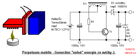
Introduction: This device is not a true perpetual motion machine or a source of free energy from the atmosphere; however, it presents an intriguing experiment, particularly for beginners and enthusiasts of alternative energy sources. It enables the generation of...
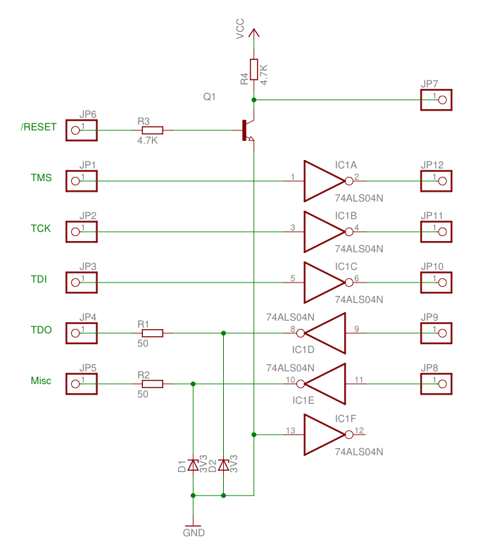
This is a quick hack on a veroboard instead of a neat PCB, but here is the schematic. Three outputs (TMS, TCK, TDI) are routed to the 74HC04 for buffering. The /RESET output directly drives a pull-down NPN transistor....
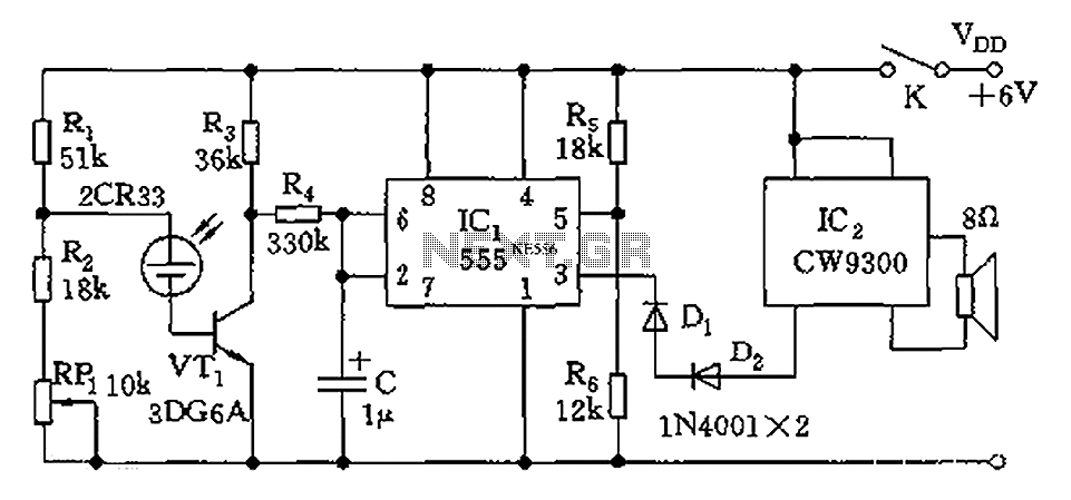
The circuit utilizes photoelectric sensors and a 555 timer to respond to music prompts. The illumination sensor components consist of photovoltaic cells (2CR33). When the light level drops below the optimal learning illumination of 100 lux, the 2CR33 exhibits...