
Integrated OTL power amplifier circuit composed by the TDA2040

The TDA2040 integrated power amplifier is designed for audio applications, providing high-quality amplification with a simple circuit configuration. The use of a +3V single supply allows for a compact design suitable for battery-operated devices. The circuit achieves a voltage gain of 30 dB, indicating significant amplification of the input audio signal, which is essential for driving speakers effectively.
The speaker impedance of 4 ohms is a standard value for many audio applications, ensuring compatibility with a wide range of speakers. The output power rating of 5W, with a potential peak of 7.5W, provides sufficient power for driving small to medium-sized speakers without distortion. The circuit's design incorporates an input coupling capacitor that isolates the amplifier from the source, preventing DC offset issues and ensuring that only the AC audio signal is amplified.
The biasing network, which includes a resistor connected to half the supply voltage, establishes the operating point of the amplifier, ensuring it functions within its linear range. This careful biasing is crucial for maintaining audio fidelity and preventing clipping during high signal peaks. The feedback network, composed of feedback resistors and capacitors, plays a vital role in stabilizing the gain and improving linearity, thereby enhancing the overall sound quality.
Vibration absorption at the output terminal is achieved through a combination of resistors and capacitors, which dampen any unwanted oscillations or ringing that may occur during operation. This feature is particularly important in audio applications where clarity and distortion-free sound reproduction are paramount. The power supply filter capacitor further ensures that any noise from the power supply does not interfere with the amplifier’s performance, providing a clean and stable voltage to the circuit.
Overall, the TDA2040 OTL power amplifier circuit is a well-engineered solution for audio amplification, balancing performance, simplicity, and component count, making it suitable for various audio applications. By an integrated power amplifier TDA2040 composed OTL power amplifier circuit is shown, which uses +3V single supply as the working voltage. This circuit voltage gain 30 dB (32 times magnification), the speaker impedance Z chaos 4 Q, output power I5W, speaker barrier anti ZBL: 80, the output power is 7.5W. In this circuit, the voltage signal by the integrated power amplifier IC-inverting input terminal of the input coupling capacitor .cl .RJ, bias resistor R2 to the inverting input terminal of the integrated circuit in the power supply voltage of i bias/2 (+16 V) .R3 role is to prevent the bias resistor R, Rz reduced input impedance .Rs feedback resistor, it C4, R4 together form the exchange of negative feedback network, the decision circuit a voltage amplification gain of the circuit RS/R4.C7 the coupling capacitor .R6, C6 form the output terminal network vibration absorption, prevent self-excited circuit .C, the power supply filter capacitor C5.
Related Circuits
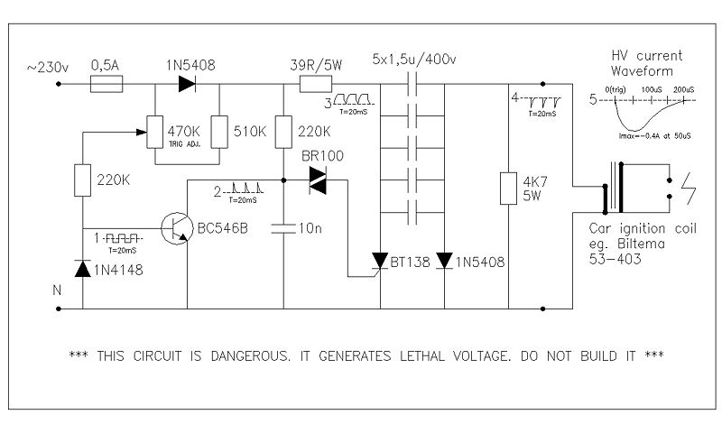
This circuit generates high voltage pulses from a 230 VAC line voltage. The drive end's swing comparator circuit was developed by the creator of this page. The working end is derived from a stroboscope trigger supply circuit. All circuits...

The input coupling capacitor allows the input signal to pass through to the grid of the tube while preventing the input source from potentially shorting the grid bias to ground. If the grid bias were shorted out, the 6AG7...
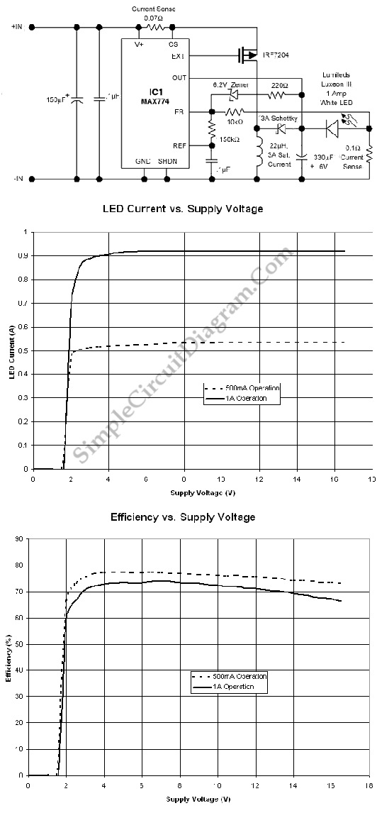
This is a high-power LED driver circuit designed to accommodate a wide input-voltage range. The circuit utilizes a buck/boost converter controller to regulate the current supplied to a white LED. The high-power LED driver circuit is engineered to effectively manage...
The schematic for the board is illustrated below. The three primary components of the board include (1) the power input and voltage regulation, (2) the L297 input and outputs, and (3) the L298 stepper motor control circuit. The motor...
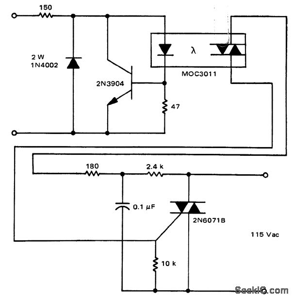
A solid-state relay circuit features an input protection mechanism utilizing the MOC3011 triac driver. The input voltage for the protection circuit can range from 3 to 30 volts DC, as noted by Motorola Semiconductor Products Inc. The solid-state relay (SSR)...
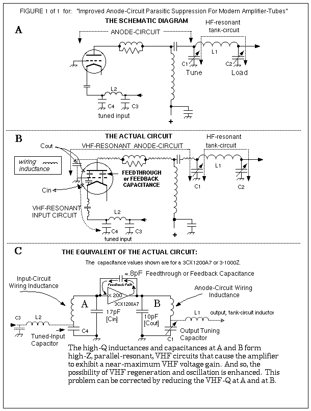
This is the unedited version of the article "Improved Anode-Circuit Parasitic-Suppression For Modern Amplifier-Tubes," which was published on page 36 of the October 1988 issue of QST. A subsequent discussion on this topic appeared in the September and October...