
Inverter size strength

The described circuit is a basic CMOS inverter consisting of a PMOS and an NMOS transistor. The PMOS transistor is connected to the positive supply voltage (V0), while the NMOS is connected to ground. When the input voltage (v1) is low, the PMOS transistor is turned on, allowing current to flow from V0 to the output, resulting in a high output voltage (5V). Conversely, when the input voltage is high, the NMOS transistor is activated, pulling the output voltage to ground (0V).
The testing procedure involves ramping the input voltage and monitoring the output voltage transition. The simulation environment provides a platform to visualize this behavior through waveforms, allowing for an analysis of the inverter's characteristics. The output waveform illustrates the inverter's logic level conversion, where the output voltage transitions from high to low as the input crosses the threshold voltage, which is found to be 2.164V in this case. This value indicates the point at which the NMOS begins to dominate the behavior of the inverter, emphasizing the difference in switching characteristics between the two types of transistors.
Understanding these characteristics is crucial for designing effective digital circuits that utilize CMOS technology, as it allows engineers to predict how the inverter will behave under various input conditions and optimize the performance of integrated circuits.The different strengths between the PMOS and NMOS transistors can be observed through a simple test of ramping up the input voltage an observing the point at which the output voltage will switch from 5V to 0V. To perform this test, click on the cell named Inverter_var_test and open the schematic view (refer to Screenshot 5).
You will notice that the circuit now consists of the inverter with some voltage sources, one providing power to the circuit (V0), one providing the input signal (v1). Now click on the Tools menu up in the top left hand corner. Then select Analog Environment and a new window will open up (refer to Screenshot 6). Now you will need to run the simulation. This is done vie either clicking on Simulation and selecting Netlist and Run or by clicking directly on the Netlist and Run button (refer to Screenshot 9).
The simulation will open up an Output Log (refer to screenshot 10) detailing the simulation while the simulation runs, and once the simulation finishes, an Output Waveform window will appear with the input and output waveforms (refer to screenshot 11). From this window (refer to screenshot 11) you will notice that as the input voltage to the inverter circuit is increased the output voltage will switch from 5V to 0V, representing a switch from a 1 value to a 0 value.
You will notice however, that the point that the output switches is not at the middle of the input range. As mentioned before, this is due to the fact the NMOS switching on more strongly than the PMOS switches off, represented as the NMOS resistance being smaller than the PMOS resistance.
The exact switching value is provided by the In->Out Cross (V) output to be 2. 164V. 🔗 External reference
Related Circuits
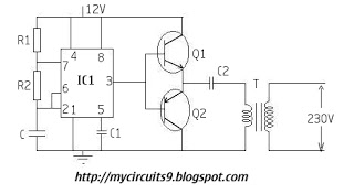
The timer IC (NE555) is configured as an astable multivibrator in this circuit. It generates an alternating non-sinusoidal output waveform as soon as a supply voltage of 12V is applied. Therefore, alternating voltage is produced from direct current (battery)....
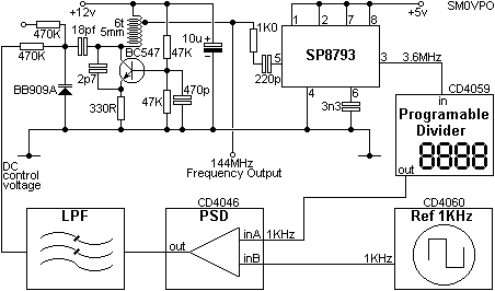
This is a programmable frequency multiplier that typically utilizes digital logic integrated circuits. The synthesizer is designed to multiply a reference frequency by a programmable factor to achieve virtually any desired frequency. For instance, with a reference frequency of...
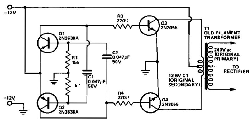
This 12 VDC to 240 VAC inverter circuit does not utilize specialized components, such as the toroidal transformer commonly found in many inverter circuits. The inverter circuit described is designed to convert a 12 VDC input into a 240 VAC...
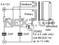
This inverter is very easy to construct, reliable, and even powerful enough to light up a 15W fluorescent tube (if you cool your transistor well). The only hard-to-find piece of this baby is the so-called yellow inverter transformer. It's...
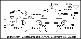
As I used this probe last night to determine if a 384 MHz oscillator was really working or not, I remembered an email I received a while ago, asking how to make a field strength indicator without the microcontroller....
This PWM control circuit generates control pulses for the DMOS power switch in the flyback circuit. The PWM output produces a pulse width that is proportional to the input control voltage, with the repetition rate governed by an external...