
Low-Drift Dc Voltmeter Circuit

The described voltmeter is an advanced measurement instrument that employs a balanced-bridge configuration using Junction Field Effect Transistors (JFETs) as the core sensing elements. The use of two matched JFETs, Q1 and Q2, is critical for achieving high accuracy in voltage measurement. The matching criterion of 10% for the drain-source saturation current (IDSS) ensures that both transistors operate under similar conditions, thereby improving the linearity and stability of the output signal.
The balanced-bridge design is particularly advantageous because it effectively cancels out common-mode noise and reduces the impact of temperature variations on the measurement accuracy. By maintaining a precise balance between the two branches of the bridge, the circuit can provide a stable output voltage that is directly proportional to the input voltage being measured. This stability is essential for applications where precision is paramount, such as in laboratory settings or high-precision instrumentation.
In terms of circuit implementation, the source-follower configuration allows for high input impedance, which is beneficial when measuring voltages from high-impedance sources without loading them down. The output of the source followers can be connected to additional signal processing stages or directly to a digital voltmeter for display.
Overall, this voltmeter design represents a sophisticated approach to voltage measurement, leveraging the characteristics of JFETs and a balanced-bridge topology to achieve reliable and accurate results across varying environmental conditions. This voltmeter uses a pair of JFETs in a balanced-bridge source-follower amplifier circuit. Q1 and Q2 should be matched within 10% for IDSS. This minimizes meter drift and maintains bridge balance over temperature.
Related Circuits
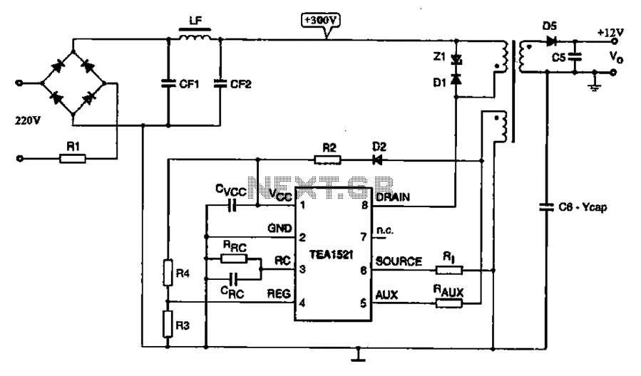
A typical DVD switching power supply circuit is shown in the standby power supply circuit of digital products. It utilizes a switching power supply structure, with the oscillation switch IC EA1623 providing oscillation pulses to the transformer. The secondary...

Drying the motor winding circuit current imbalance. Below is a circuit diagram of the motor winding current imbalance drying. The circuit for drying motor winding current imbalance is designed to address the issue of uneven current distribution across the windings...

The TDA8358J application circuit is designed for television signal processing. The input signals are connected to the TDA8358J at pins 1 and 2, where pin 1 receives a positive sawtooth voltage input and pin 2 receives a negative sawtooth...
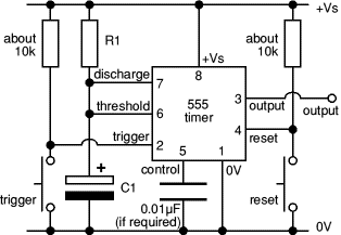
The 8-pin 555 timer is one of the most versatile integrated circuits (ICs) available, utilized in numerous projects. With minimal external components, it can be employed to construct various circuits, many of which do not pertain to timing applications....
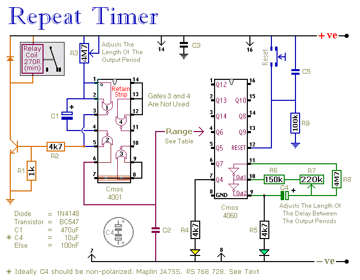
This circuit features an adjustable output timer capable of re-triggering at specified intervals. The output duration can range from a fraction of a second to over half an hour, with the ability to recur at regular intervals spanning from...

Another application involves the use of a NE555 delay lamp circuit, where components SB1 and SH2 act as J-light buttons that can be installed in two different locations. The lamp can be activated by pressing either SB1 or SB2,...