
Op amp circuit diagram relay delay release

The delayed release operational amplifier relay circuit employs an operational amplifier configured to act as a comparator. The inverting terminal receives a reference voltage through a 4.7k resistor, while the non-inverting terminal is connected to a charging capacitor (C1) that influences the output state of the op-amp. The timing mechanism is governed by the RC time constant formed by the resistor (1.2M) and the capacitor (C1), where the charge time of C1 determines the delay before the relay is activated.
When the circuit is powered, the capacitor C1 starts charging, and the voltage across it increases gradually. The operational amplifier's output remains low until the voltage across C1 exceeds the reference voltage present at the inverting terminal. At this point, the output of the operational amplifier transitions to a high state, activating the relay.
The relay can be utilized for various applications, such as controlling higher power devices or signaling alarms, depending on the load connected. The adjustable resistor (1.2M) allows for customization of the delay, making this circuit suitable for applications requiring precise timing control. The design ensures that the relay remains inactive during the charging phase of the capacitor, thereby preventing premature activation. Overall, this circuit is an effective solution for applications requiring a delay in relay activation. As shown in FIG relay the delayed release operational amplifier circuit. When the power switch, the inverting input terminal of the operational amplifier is added resistor 4.7k and 10k partial pressure of VT, C1 had a chance to charge the non-inverting input is applied low. Therefore, the operational amplifier output is low and relay. And the power to charge the capacitor through resistor 1.2M C1. With the charging capacitor C1, the voltage which is gradually increased over a period of time on the Cl voltage becomes high, so the non-inverting input plus is high, the operational amplifier output is high, the relay It is released. So this circuit is a relay delay release circuit. The length of the delay time can be varied by adjusting the 1.2M resistance, such as by the parameter map, the delay time is about 260s.
Load circuit may be a relay or solenoid coil may be lights and other display and alarm devices.
Related Circuits
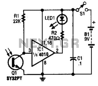
The IR Tester circuit indicates whether the button pressed on a remote control is functioning. Q1 is a phototransistor that is activated by infrared (IR) energy. The IR Tester circuit operates by detecting infrared signals emitted by remote control devices...
Circuit for Grundig 5441 TV. If there are any issues related to this circuit, please provide additional information about the problem for further assistance. By accessing the Fixya site, users acknowledge that they have read and agreed to its...
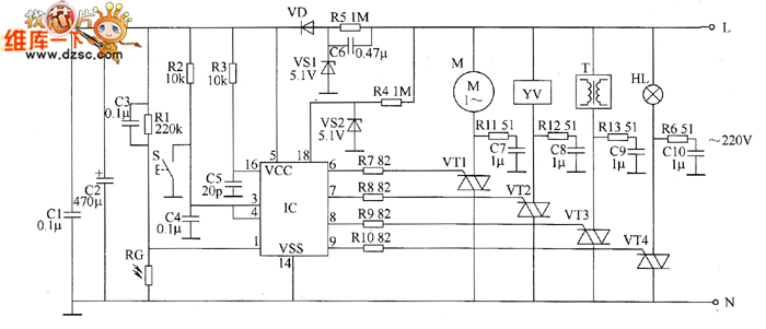
The industrial fuel oil furnace controller circuit consists of a power supply circuit, a testing and ignition control circuit, and a control implementation circuit, as illustrated in the accompanying diagram. The power supply circuit includes a step-down capacitor (C6),...
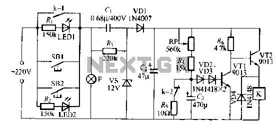
The lamp relay delay circuit is illustrated in Figure 7. Components S131 and SB2 are light buttons mounted in different locations. The lamp can operate with F. LEDs (LED1 and LED2) should be installed in SB1 and SB2 to...
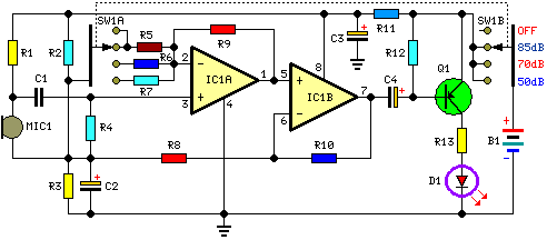
This circuit is designed to indicate when room noise exceeds a predetermined threshold, utilizing a flashing LED to signal this condition. Three fixed noise levels are selectable: 50 dB, 70 dB, and 85 dB. The circuit employs two operational...
This circuit was originally a type of power-delay control circuit, where the delay time is determined by the timing elements R1 and C1. Additionally, with the inclusion of a "watchdog" circuit, it can be utilized as a monitoring circuit...