
Rf probe for vtvm

The circuit operates based on the principles of pulse width modulation (PWM) and voltage regulation. The 555 timer is configured in astable mode, which allows it to generate a square wave output. The frequency of this output is determined by the timing components, including the external potentiometer and the capacitor. The 2N2222 transistor acts as a switch that controls the flow of current through the load based on the varying control voltage from the 555 timer.
In this configuration, the external potentiometer serves as a variable resistor that adjusts the base current of the 2N2222 transistor. As the resistance of the potentiometer changes, it modifies the voltage at the base of the transistor, which in turn alters the collector current flowing through the load. This change in collector current affects the output voltage, providing a means to achieve the desired voltage level.
The use of a 1 kΩ resistor in the collector circuit ensures that the transistor operates within its safe limits while allowing sufficient current to flow to the load. The 3 µF capacitor plays a critical role in smoothing out the output voltage, filtering the rapid changes caused by the PWM signal generated by the 555 timer. This capacitor charges and discharges in response to the switching of the transistor, effectively stabilizing the output voltage.
The output voltage range of 0 to 10 V is suitable for various applications, and the regulation specifications ensure that the circuit can maintain a stable output even when the load current varies. The design is efficient and can be used in applications requiring precise voltage control, such as in power supplies for sensors or actuators. Overall, this circuit exemplifies a practical application of basic electronic components to achieve effective voltage regulation with minimal complexity.This circuit combines a 555 timer with a 2N2222 transistor and an external potentiometer. The pot adjusts the output voltage to the desired value. To regulate the output voltage, the 2N2222 varies the control voltage of the 555 IC, increasing or decreasing the pulse repetition rate. A 1 K resistor is used as a collector load. The transistor base is driven from the external pot. If the output voltage becomes less negative, the control voltage moves closer to ground, causing the repetition rate of the 555 to increase, which, in turn, causes the 3 µf capacitor to charge more frequently
Output voltage for the circuit is 0 to 10 V, adjusted by the external pot. Output regulation is less than five percent for 0 to 10 mA and less than 5 percent for 0 to 0 mA.
Related Circuits
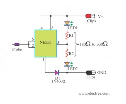
This circuit allows users to determine whether a specific point in the circuit is at a positive or negative voltage. It is an inexpensive circuit that utilizes minimal components, making it suitable for use in automobiles or motorcycles. The...
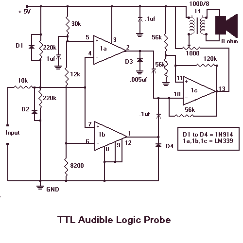
When testing circuits with a logic probe, it is sometimes difficult to watch the LEDs on the probe to determine the logic state. With this probe, the logic states are audible. This probe is designed for TTL circuits only...
The probe indicates a high or low state at 70% and 30% of the supply voltage (V+), which ranges from 5 to 12 V. One section of the voltage comparator (LM393) detects when the input voltage exceeds 70% of...
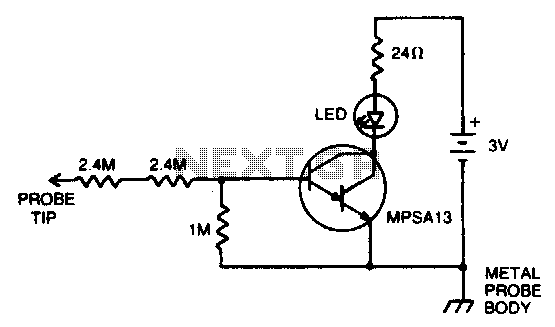
Insert the probe tip into either terminal of an AC outlet and hold the probe body against any object that the circuit ground is connected to. The LED will illuminate when the hot terminal is touched. Two 2 MΩ...
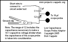
The capacitance between the wire and the probe would form a capacitive voltage divider with the probe's input capacitance, and at frequencies significantly higher than the low frequency roll off created by the probe's input capacitance and the probe's...
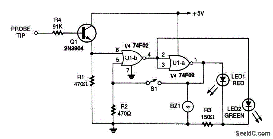
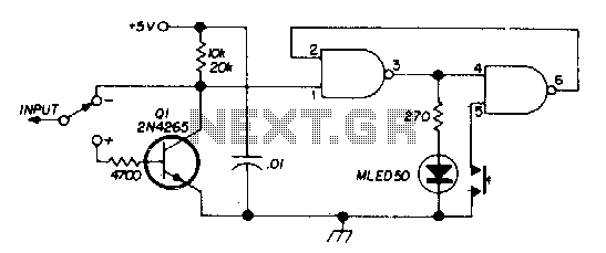
This logic probe includes high-low (LED) indication and a latching operation. When switch S1 is closed, the pulse indication is latched, causing the red LED1 to remain illuminated. A piezoelectric buzzer, BZ1, serves as an audible indicator to signal...