
Simple RS 232 Level Converter

The RS-232 converter circuit designed by Wichit Sirichote is a practical solution for interfacing microcontrollers with serial communication ports on PCs. The circuit primarily consists of two transistors: a PNP transistor (BC557) for the transmitter and an NPN transistor for signal reception. The operation of the transmitter circuit is crucial for ensuring proper voltage levels are maintained during data transmission.
In the transmitter section, when the TxD signal is logic '1', the PNP transistor Q1 is turned off, resulting in a negative voltage output of approximately -9V at the RxD pin. This is in accordance with the RS-232 standard, which defines a logic '1' as a negative voltage. Conversely, when the TxD signal transitions to logic '0', Q1 is activated, allowing a positive voltage of about +5V to be sent to the RxD pin. This voltage level corresponds to a logic '0' in the RS-232 protocol.
The dashed line in the circuit diagram indicates the separation between the transmitter and receiver sections, which allows for independent operation. Users who require only the transmitter functionality can utilize this design without needing the receiver part. The circuit is straightforward, making it suitable for hobbyists and professionals seeking an efficient and economical way to implement RS-232 communication in their microcontroller projects.
Overall, this RS-232 converter circuit serves as a reliable interface for microcontrollers, enabling effective communication with PC COM ports while adhering to the necessary voltage levels defined by the RS-232C standard. By employing simple components like the BC557 transistor, it provides an accessible solution for various electronic projects.When you need connect your Microcontroller Project to COM port in PC you need RS 232 converter. There are many chip to solve the problem like MAX232, DS275 etc. But if you need simple and chep for RS 232 converter, i though this circuit will be usefull for you. The design made by Wichit Sirichote. "A circuit diagram shown above was used two small signal transistor, NPN and PNP transistors. Dash line separate transmitter and receiver circuit. For those who need only transmitter circuit can use above circuit (and GND (5) signal ). Technically the RS232C is -3V to -12V for logic `1` and +3V to +12V for logic `0`. The transmitter circuit uses PNP transistor, BC557. While in mark state the TxD signal is logic `1`, Q1 turns off. TxD (pin3) then provides -9V (depends on what converter chip being used for COM1, say) to RxD (pin2). For space state, TxD control signal then becomes logic `0`, which turns on Q1, the approx. +5V is then fed to RxD (pin2). With this method, while sending data has being made, TxD (pin3) must stable at -9V, say" 🔗 External reference
Related Circuits
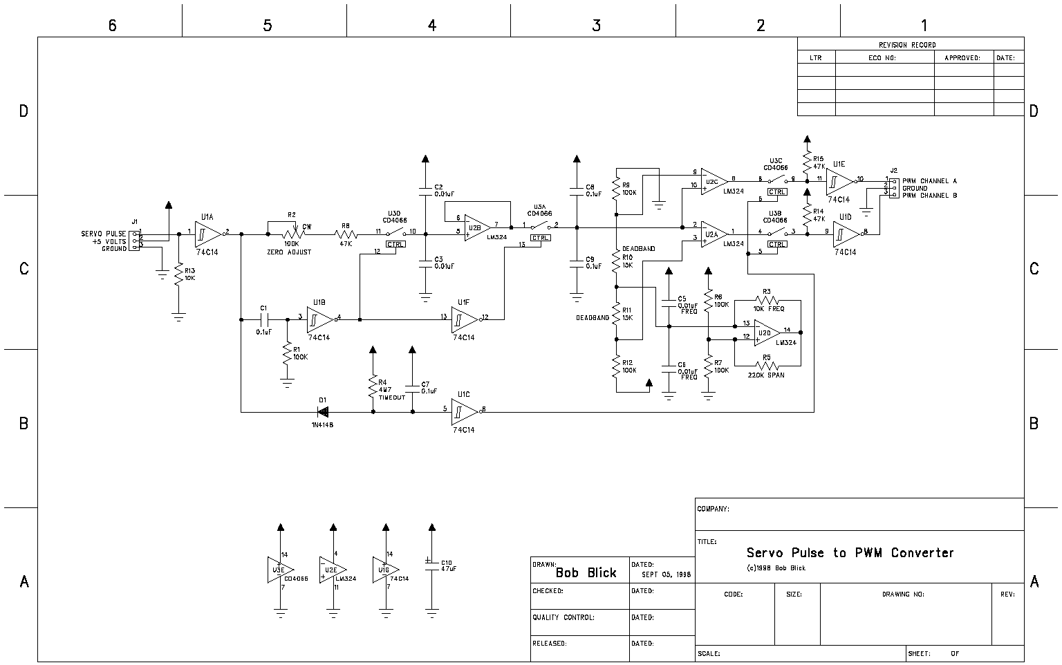
The circuit presented on this page attempts to be an interface to convert pulses such as provided by a Basic Stamp or R/C receiver to a dual PWM (Pulse Width Modulation) signal required by an H-bridge. The simplest circuit...
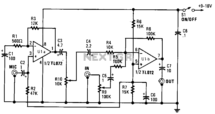
This mixer is constructed using a TL072 dual BiFET operational amplifier featuring a JFET input stage and can be powered by a single-ended power supply ranging from 9 to 18 volts. The microphone input is capacitively coupled to the...
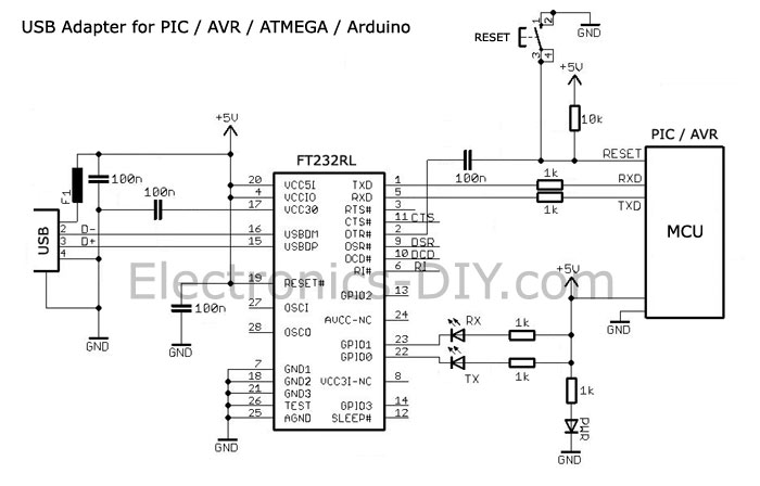
The FT232RL USB to Serial UART (TTL) Adapter is an affordable and straightforward solution for connecting PIC, AVR, or ATMEGA microcontrollers to a PC or Mac via a USB interface. The FT232RL chip is noteworthy for its compliance with...

With the component values shown, the oscillator has a frequency of 8 kHz. When an input signal is applied to the base of Q1, the current flowing through Q1 is varied, thus affecting the time required to charge C1....
This design idea explains how to develop a water sensor circuit that can monitor upper and lower water levels. The water sensor circuit is designed to detect and monitor water levels within a specified range, providing feedback when the water...
This is likely the simplest radio transmitter available, consisting of five components and capable of being assembled in a compact space. It is suitable for science fair projects or other science-related endeavors where short-range transmission is beneficial. The device...