
Single Supply Function Generator

In this circuit, R1 and R2 play a crucial role in shaping the amplitude of the triangle wave generated. The relationship between these resistors dictates how high or low the triangle wave will oscillate, directly influencing the output characteristics when compared to the square wave. The triangle wave's amplitude is critical for applications that require precise waveform characteristics, such as in signal processing or modulation techniques.
The frequency of oscillation is determined by the equation provided, where R3 and C1 are additional components that help define the timing characteristics of the circuit. R3 is a resistor that, in conjunction with the capacitor C1, sets the time constant for the charging and discharging cycles that produce the oscillation. The factor of 4 in the denominator indicates that the frequency is inversely proportional to the product of R3 and C1, meaning that increasing either component will decrease the frequency of oscillation.
This configuration allows for flexibility in tuning the circuit to achieve desired waveform frequencies and amplitudes. The ratio of R2 to R1 allows for further fine-tuning of the triangle wave's amplitude, which can be essential in applications such as waveform generation, signal modulation, and audio synthesis. By adjusting these resistors, one can achieve a wide range of output characteristics suitable for various electronic applications.
Overall, the interplay between R1, R2, R3, and C1 is fundamental in designing circuits that require precise waveform generation, making this configuration valuable in both educational and practical electronic engineering contexts.The ratio R1/R2 sets the amplitude of the triangle wave, as referenced to the square-wave output. For both waveforms, the frequency of oscillation can be determined by the equation: fo= 1/4R3C1 * R2/R1 🔗 External reference
Related Circuits

Transformerless Power Supply Circuit Diagram. The selection of the dropping capacitor and the circuit design requires technical knowledge and practical experience to achieve the desired voltage and current. The transformerless power supply circuit is a compact and efficient solution for...
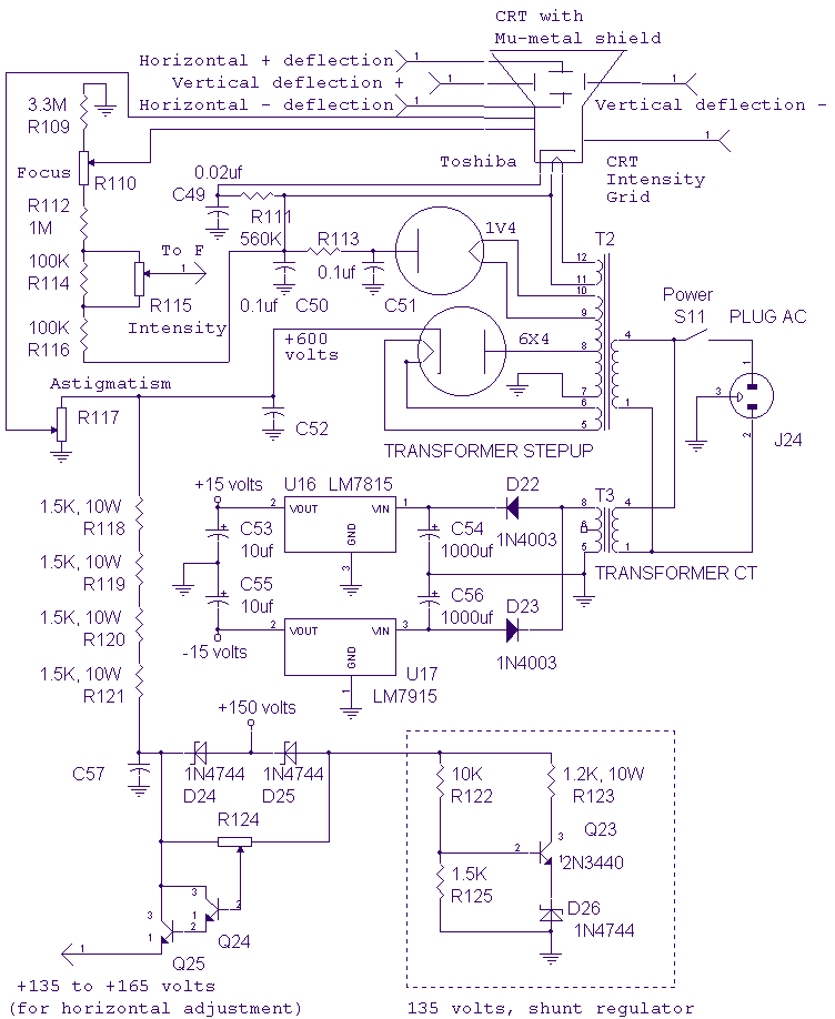
The high voltage section of the CRT is unchanged from the original vacuum tube oscilloscope used as the basis of this design. The CRT requires shielding from the main power transformer. Cold roll steel around the CRT does not...

A single-phase rectifier DC welding power load from the road circuit is presented. The contactor KM utilizes a CJ20-40A model rated for 220V. An adjustment potentiometer RP is employed to ensure proper arcing, while the relay KA2 is designed...

40V regulated power supply based on TIP42A and LM317. Refer to the specified page for an explanation of the related circuit diagram. The 40V regulated power supply utilizes a TIP42A transistor and an LM317 voltage regulator to provide a stable...
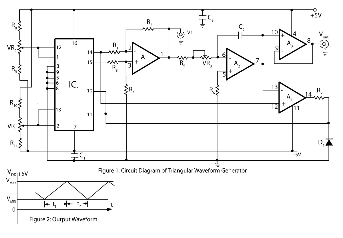
The triangular wave generator featured on this website offers significant advantages, including a circuit diagram and a detailed description of its operation, focusing on achieving maximum and minimum peak levels of the triangular wave. The triangular wave generator is an...

The circuit was designed to create a frequency generator that consists of seven steps during operation. It includes a crystal oscillator, which is an electronic circuit made of... The frequency generator circuit operates through a series of seven distinct steps,...