
switching power supply 4

The MAX1846 and MAX668 circuits are designed to efficiently convert input voltages to desired output levels while maintaining stability and minimizing noise. The integration of filtering components, such as capacitors and resistors, is crucial for ensuring that high-frequency noise does not interfere with current sensing and regulation. The use of controlled slew rates and internal compensation mechanisms demonstrates advanced engineering techniques aimed at enhancing the performance of switch-mode power supplies. Furthermore, the incorporation of additional circuitry, such as the CD4093 and CD40106, showcases the versatility of these designs, allowing for voltage multiplication and high-voltage generation in compact configurations. The choice of components, including the 7555 timer and the stroboscope transformer, highlights the importance of selecting suitable elements for specific applications, ensuring reliability and efficiency while achieving the desired electrical characteristics.The MAX1846 inverting circuit to implement a switch-mode power supply that provides a -15V at 0. 5A output from a 4. 5V to 12V input. This MAX1846 circuit also adds a few components to the minimum circuit implementation. C20 adds a pole to compensate for the ESR-zero of the output capacitor, while R16 and C22 filter the current-sense voltage to prev ent high-frequency switching noise from tripping the current limit. This functionality is in addition to the MAX1846 ²s internal 100ns current-sense blanking time. The MAX1846 EXT pin implements controlled slew rate, which helps limit high-frequency switching noise. The MAX668 boost circuit to implement a switch-mode power supply that provides a +15V at 0. 5A output from a 4. 5V to 12V input. This MAX668 circuit adds a few components to the minimum circuit implementation. C7 adds a pole to compensate for the ESR-zero of the output capacitor. R5 and C8 filter the current-sense voltage to prevent high-frequency switching noise from prematurely tripping the current limit.
This functionality is in addition to the MAX668 ²s internal 60ns current-sense blanking time. The MAX668 output voltage can be changed to +12V by changing the value of the R2 resistor to 86. 6k This change reduces the minimum input voltage to approximately 10V. Since the MAX668 provides internal compensation, no other changes are required for +12V output. The output ripple voltage due to switching can be reduced an order of magnitude with a secondary output filter set to one-tenth of the switching frequency. A 1, 0. 5W resistor in series with a 10uF, 25V capacitor with less than 100m ESR introduces a 0. 5V decrease in output voltage at a 0. 5A load. The feedback voltage must be sensed before it reaches the secondary filter for the MAX668 to maintain stability.
If you have power supply source about 12V, from battery 4A sizes. But want to enhance voltage be 24V or about 2 times. This circuit has can to help you by it has prominent easy good point. It use the integrated circuit digital number CD4093 perform produce the frequency drive current change CD40106 bilateral the group trips work. By drive high current with power mosfet BUZ11 make output current collect at capacitors the very total up voltage bilateral the group then is double of Input power supply.
or It can enhance voltage double, be 2 times there. The circuit can be used to generate a voltage of about 70V using a current of about 4 mA @ 6V input voltage. The use of an easily available stroboscope trigger coil makes it quite small. The integrated circuit is a 7555 generating a 50/50 square wave of around 100 kHz. The square wave`s rising edges momentarily trigger the transistor into conduction, causing current to flow through the primary of the stroboscope transformer.
The current pulse in the primary causes a much larger voltage pulse in the secondary of the transformer, thereby charging the output capacitor through the diodes. I`m using the 7555 (CMOS variety of the NE555) to generate the square wave, because it behaves much better with respect to power supply transients than the NE555.
The circuit topology used here makes it possible to generate a 50% duty cycle square wave with only few external components (the resistors from output to treshold/trigger and the capacitor between treshold/trigger and ground). The type of transistor is not very important I think. I just used a BC550 because I had it available. On the rising edge of the square wave, the transistor is switched on through the capacitor. It is quickly switched off, because the capacitor discharges through the resistor between base and ground.
I connected a diode across the transistor`s emitter and collector, to protect it against the negative voltage spike from the primary winding. The stroboscope trigger coil is a 4 kV type, meaning that it is supposed to convert a 300V pulse to 4 kV in its original application (a step-up ratio of ab
🔗 External reference
Related Circuits
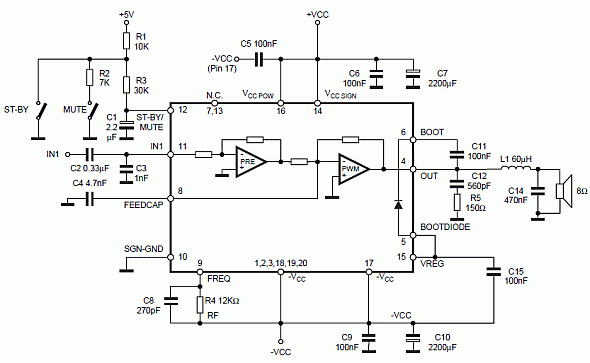
Class D audio power amplifier schematic diagram with TDA7480, capable of 10W output power at a load of 8Ω/4Ω and a total harmonic distortion of 10%. Requires a split-supply (max. ±20V). The Class D audio power amplifier utilizing the TDA7480...
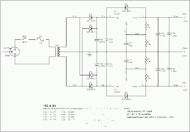
This document describes how to construct a dual polarity linear power supply which can be configured for any positive or negative voltage between 1.2-35V. A power supply is the fundamental building block of all but the simplest of electronic...
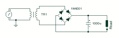
A basic full wave rectified power supply is shown below. The transformer is chosen according to the desired load. For example, if the load requires 12V at 1amp current, then a 12V, 1 amp rated transformer would do. However,...
This circuit functions as an ultra-low power alternative to multiple LED on-off indicators. It is designed to be easily readable in full daylight conditions. The described circuit employs a low-power microcontroller or a dedicated LED driver IC that manages the operation...
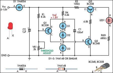
This is a simple low supply rail detection circuit that is inexpensive and can be assembled in approximately 20 minutes. Its low power consumption makes it suitable for integration into battery-powered devices. Instead of utilizing an operational amplifier, the...
Stationary - MOPLL & Silicon Tuner TUA6020 2 Band TV Tuner Mixer-Oscillator-PLL with balanced IF-Amplifier. The TUA6020 device integrates a digitally programmable Phase Locked Loop (PLL) with a mixer-oscillator block that includes two balanced mixers and oscillators suitable for...
Warning: include(partials/cookie-banner.php): Failed to open stream: Permission denied in /var/www/html/nextgr/view-circuit.php on line 713
Warning: include(): Failed opening 'partials/cookie-banner.php' for inclusion (include_path='.:/usr/share/php') in /var/www/html/nextgr/view-circuit.php on line 713