
The camera flashlight circuit

The camera flashlight circuit is designed to provide a reliable illumination source for photography applications. The operation begins with the closure of switch K1, which engages the self-oscillating circuit. This circuit is essential for generating a high-frequency signal, which is facilitated by the components BG1 (a transistor), C1 (a capacitor), B1 (a battery), and R1 (a resistor). The oscillator's output is then amplified by the battery B1 and converted to a usable form through diode D1, which rectifies the AC signal to charge capacitor C2.
Once C2 is sufficiently charged, diode DW2 plays a critical role by allowing current to flow when the voltage reaches 5.6V. This action activates transistor BG4, which is pivotal for the subsequent multi-resonance oscillator stage. The multi-resonance oscillator is composed of transistors BG2 and BG3, along with a network of resistors (R3 to R7) and capacitors (C3 and C4). This configuration is designed to produce a stable and consistent flash signal of 2.5V, which is crucial for the flashlight's operation.
The overall design ensures that the circuit can efficiently convert stored energy into a powerful flash, making it suitable for various lighting conditions in photography. The use of multiple oscillators and rectification stages enhances the reliability and performance of the flashlight circuit, ensuring that it meets the demands of high-speed photography and low-light environments.The camera flashlight circuit when K1 is put through, the self-motivation oscillator composing of BG1, C1, B1 and R1 is starting to work, after being boosted by B1 and rectified by D1, it is charging C2. DW2 makes BG4 conduct when it is 5.6v, the multi-resonance oscillator composed of BG2, BG3, R3~R7, C3 and C4 is getting into working, the 2.5V flash signal..
🔗 External reference
Related Circuits
This circuit will filter out interference signals and ensure that the signal received from the Morse code station stands out. The described circuit functions as a signal processing system specifically designed to enhance the clarity of Morse code transmissions by...

This basic tuned LC amplifier can be used with three output coupling methods: capacitive coupling output, capacitive tapped output, or link-coupled output. The tuned LC amplifier is a fundamental circuit used in various applications, including radio frequency (RF) amplification and...
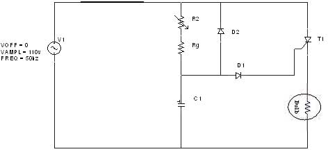
The diagram illustrates an R-C-Diode circuit that provides full half-cycle control (180 electrical degrees). During the positive half-cycle of the SCR anode voltage, the capacitor charges to the trigger point of the SCR, a process governed by the RC...
This site serves as a collection of useful information that the author wishes to retain, with the occasional inclusion of pages that may be of interest to others. The author has documented the retrofit of the Boxford 125 TCL...
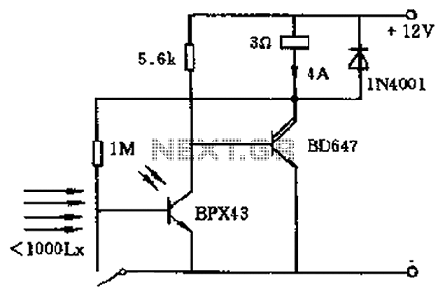
In the circuit's resting (dark) state, current flows through the electromagnet M. When light shines on the phototransistor, it turns on, causing the final stage transistor to enter the OFF state, which releases the solenoid. A 1M ohm feedback...

Pressing the START pushbutton activates either the headlights or spotlights for a specified duration. After 1 minute, determined by R1 and C1, the lights will turn off as the NE555 timer completes its cycle. The circuit utilizes a NE555 timer...