
The frame memory circuit

The digital signal processing (DSP) circuit is designed to facilitate efficient image data handling through a structured memory architecture. The DPTVT-3D/MV chip serves as the core processing unit, interfacing with four KM416S102 memory chips, each capable of storing 16 MB of data. The arrangement allows for a total of 64 data lines, which enables the DSP to manage large volumes of image data in parallel, enhancing processing speed and efficiency.
The memory units are connected to the DPTVT-3D/MV chip via 16 data lines per unit, facilitating simultaneous data transfer across multiple channels. This parallel configuration is crucial for applications requiring high-speed data processing, such as real-time image analysis or video processing. Each memory unit is also equipped with 10 address lines, which are essential for accessing specific memory locations within the chip. This addressing capability allows the DSP to retrieve and manipulate data efficiently, ensuring that the required information is available when needed.
Furthermore, a common control bus connects all memory units to the main DSP chip, allowing for coordinated control signals to manage read and write operations across the memory modules. This architecture not only streamlines data flow but also simplifies the control logic required for memory management, making the circuit more robust and easier to integrate into larger systems. The overall design emphasizes modularity and scalability, making it suitable for various digital signal processing applications that demand high performance and reliability.Digital signal processing circuit when work needs to cooperate with it with a memory for temporarily storing image data. DPTVT-3D/MV digital processing chip need four KM416S102 0B (16 MB) digital memory and it is coupled, the circuit structure shown in Figure 26-6, only one is drawn out of the two pieces (U5, U6), the remaining two (U7, U8) is not successful in the drawing. Each memory has 16 lines, or 16-bit parallel data and digital processing chip DPTVT-3D/MV is connected to access a data signal, a total of 64 lines.
In addition, each memory has 10 lines (to address signal) is connected to the main digital signal processing chip, in addition to the common control bus
Related Circuits
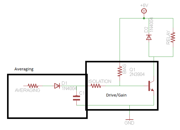
A circuit that activates a relay upon detecting audio pulses from one channel of an MP3 player. The intention is to synchronize recorded audio pulses with music to control a motor for mouth movement. For a stereo player, music...
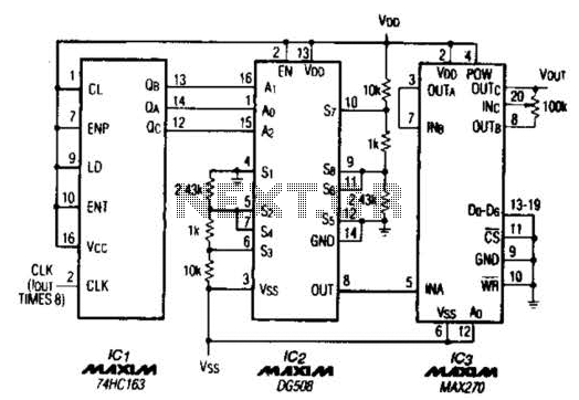
A TTL counter, an 8-channel analog multiplexer, and a fourth-order low-pass filter can generate sine waves ranging from 10 kHz to 25 kHz with a total harmonic distortion (THD) better than -80 dB. The circuit employs two cascaded second-order,...
This circuit employs switched emitter followers instead of conventional analog switch CMOS chips, resulting in a more effective reduction of crosstalk between channels. It can manage up to 4 Vms with less than -80 dB crosstalk. The circuit design utilizes...
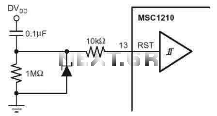
According to the MSC1210 datasheet, you will perform an external reset by taking RST pin high for two tOSC periods as this stops device operation, crystal oscillation, causes all digital pins to be pulled high from that point and...
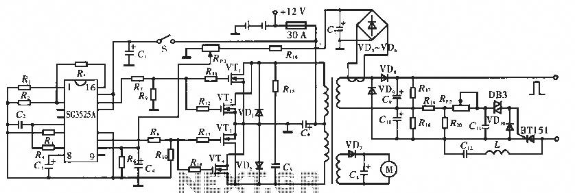
The circuit utilizes the SC3525A, a PWM silicon chip from US General Semiconductor. It features an error amplifier with an inverting input at pin 1. Pin 2 serves as the non-inverting input for the error amplifier. Pins 5 and...
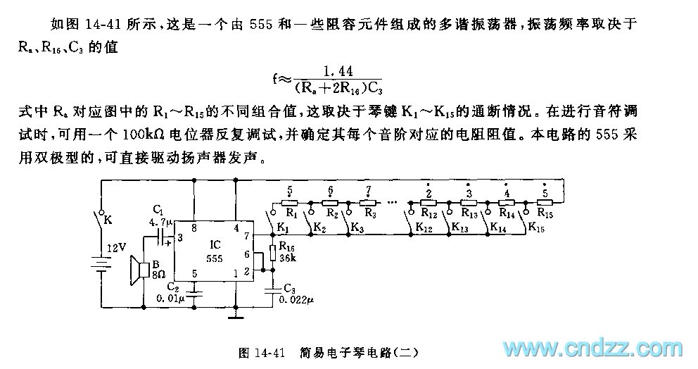
Figure 14-41 illustrates a multivibrator circuit utilizing a 555 timer alongside various capacitive and resistive components. The oscillation frequency is determined by the values of Ra, R16, and C3, following the formula f = 1.44 / ((Ra + 2R16)...