
The second equalization circuit

In this circuit configuration, the potentiometer serves a critical role in adjusting the feedback path, which directly influences the gain characteristics of the equalization circuit. The feedback resistor RB is strategically placed in parallel with the input resistance lc to form a dynamic resonance impedance that can be fine-tuned through the potentiometer. This design allows for precise control over the frequency response of the circuit, enabling it to adapt to various audio signals or other input waveforms.
The maximum gain achieved when the wiper is positioned at the inverting input terminal "a" indicates that the circuit is optimized for a specific frequency fo, where the resonance condition is met. This configuration is particularly useful in audio processing applications, where enhancing certain frequencies can lead to improved sound quality.
On the other hand, adjusting the wiper towards the inverting input terminal "+" results in a minimum attenuation scenario. This adjustment effectively reduces the signal gain, which can be beneficial for preventing distortion or clipping in high-amplitude signals. The ability to manipulate the gain through the potentiometer provides versatility in tuning the circuit to achieve the desired audio characteristics.
Overall, the second equalization circuit connection method exemplifies the delicate balance between feedback and gain, showcasing how component placement and adjustment can lead to significant changes in circuit performance. This understanding is crucial for engineers designing audio equipment or other signal processing devices that require precise control over frequency response and gain settings.In the second equalization circuit connection method, and it works as shown in Figure 1-96. When the potentiometer wiper is moved lc inverting input terminal "a", the resonance impedance of the parallel combination of the feedback resistor R B is the minimum, the minimum amount of feedback and thus, the maximum gain of the circuit, corresponding to the frequency o and around the gain obtained promotion. When the potentiometer wiper move lC-inverting input terminal "+", the B input and lc R'o parallel resistance value of the minimum attenuation, so that the amount and rate of around fo signal input into the minimum voltage gain is attenuated.
Related Circuits

This circuit converts a sine wave into a square wave. It consists of a single 2-input NAND Schmitt trigger configured as an inverter, with an adjustable trigger level at its input. As the input voltage exceeds the gate's trigger...
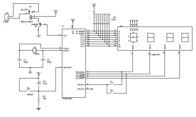
The circuit diagram above illustrates the Clock Controller V1.1. Pins P3.0 to P3.3 are connected to the base of a 4-PNP transistor, specifically the 2N2907, which is used to sink current. The Clock Controller V1.1 circuit is designed to manage...
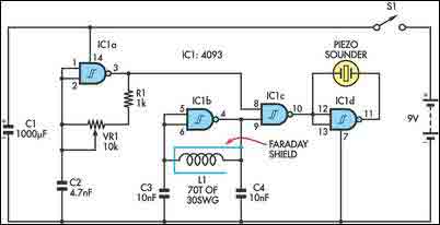
The circuit incorporates two oscillators, both operating at about 40kHz. The first, IC1a, is a standard CMOS oscillator with its frequency adjustable via VR1. The frequency of the second, IC1b, is highly dependent on the inductance of coil L1,...
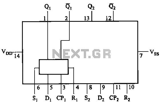
The CD4013 is a dual D flip-flop that operates on the rising edge of the clock signal. Its internal block diagram and pin configuration are provided. This device is part of the standard model C043 and the GB model...
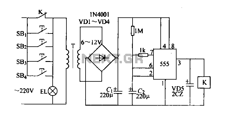
Control buttons SB1 to SB4 can be installed in various positions within a corridor. By pressing any one of these buttons, the EL horse lights will turn on. After releasing the button, the transformer and rectifier supply power to...
With switch SI in the off position, battery voltage is applied across timing capacitor CI, which remains charged while the rest of the circuitry is powered off. Transistor Q1, and consequently transistors Q2 through Q4, remain in an off...