
TTL Three - State Logic Probe PCB

The TTL logic probe circuit using the HD74LS00 quad-NAND IC is designed to provide clear visual feedback regarding the logic levels present in a digital circuit. This probe operates in three distinct states: high, low, and high impedance (three-state operation), which allows the user to determine the state of a digital signal without significantly affecting the circuit under test.
The configuration of Gate N1 is critical for indicating a high logic state. When the input to Gate N1 is at logic 1, the output transitions to logic 0, which in turn activates LED1. This visual cue is essential for technicians and engineers as it indicates that the point being probed is at a high state, essential for diagnosing digital circuits.
Conversely, Gate N3 is configured to illuminate LED3 when its output goes high, indicating that the point being tested is at a logic 0 level. This dual-indicator system allows for quick and efficient troubleshooting, as the user can easily ascertain whether a signal is high or low at a glance.
In the implementation of this circuit, the choice of the HD74LS00 IC is particularly advantageous due to its low power consumption and fast switching times, which are beneficial in high-speed digital applications. The use of diodes D2, D3, and D4 further enhances the circuit's flexibility, allowing for compatibility with various other TTL families, ensuring that the logic probe can be adapted for use with different integrated circuits as necessary.
Overall, this TTL logic probe circuit is a powerful tool for digital circuit analysis, providing essential functionality in a compact form factor, making it invaluable for engineers and technicians working in electronics.A TTL logic probe is an indispensable tool for digital circuit troubleshooting. Various methods can be used to design a logic probe. The most common designs employ opamps, logic (OR, NOT, XOR) gates, and transistors. The circuit presented here uses NAND logic gates of Hitachi HD series IC HD74LS00, which is a quad-NAND IC. Special technique has be en employed to obtain three-state operation using just a single IC. In the circuit Gate N1 is wired such that when the output of gate N1 is at logic 0` (i. e. when its input is at logic 1`), LED1 will glow, to indicate high state of the point being probed. Gate N3 is wired to light LED3 when the output of gate N3 is high or when the point being tested is at logic 0` level. At power-on, the output of If any other type of IC (e. g. 74HCT00 or 74LS00) is used, diodes D2-D3-D4 should be added or deleted as necessary; for example, when using HD74LS00, one diode D2 is required.
🔗 External reference
Related Circuits
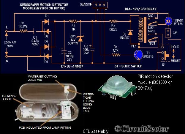
This circuit diagram is based on the PIR motion sensor module BS1600 (or BS1700) designed for security lighting in power-saving mode. If the component is unavailable in local stores, it can be purchased online. A key advantage of this...
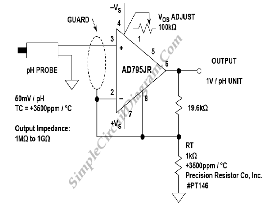
A buffer amplifier is necessary for a typical pH probe to isolate its source resistance, which ranges from 10^6 to 10^9 ohms, from the external circuitry. Such an amplifier is illustrated in the... The buffer amplifier serves a critical role...
The differential outputs are balanced and designed to drive long lengths of coaxial cable, stripline, or twisted pair transmission lines with characteristic impedances ranging from 50 ohms to 500 ohms. Differential transmission is superior to single-wire transmission as it...
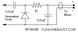
An RF probe is used to directly measure the level of RF voltage present at a particular point and is one of the most useful test instruments in the hands of the home brewer. It is normally used with...
TL072 is a low-noise JFET input operational amplifier characterized by features such as a common-mode input voltage range, high slew rate, operation without latch-up, compensated internal frequency, high input impedance at the JFET input stage, low noise, low total...
This circuit is designed to demonstrate high frequency and high voltage, capable of producing up to approximately 30 kV, depending on the transformer utilized. It is an economical and straightforward project, primarily using a standard TV flyback transformer. The...