
Typical DA conversion circuit 8

The D/A conversion circuit depicted employs the DAC0830/DAC0832, which is a dual 8-bit digital-to-analog converter. This device is designed to convert binary input signals into corresponding analog voltages, facilitating the interface between digital systems and analog environments.
The circuit typically includes a microprocessor that generates an 8-bit digital signal, which serves as the input for the DAC. The DAC0830/DAC0832 interprets this digital input and outputs an analog voltage proportional to the digital value. The output voltage can range from 0 to a maximum value determined by the reference voltage supplied to the DAC, allowing for precise control over the analog signal produced.
In addition to the DAC chip, the circuit may incorporate passive components such as resistors and capacitors to filter the output signal and stabilize the power supply. A reference voltage source is also essential, as it sets the scale for the output voltage range. The circuit configuration may vary depending on the desired application, such as audio signal generation, waveform synthesis, or control systems.
To ensure optimal performance, it is crucial to consider factors such as the power supply voltage, load impedance, and signal integrity. Proper layout and grounding practices are also important to minimize noise and ensure accurate signal conversion. Overall, the DAC0830/DAC0832 provides a reliable solution for converting digital signals into analog outputs in various electronic applications.8 shows a typical D/A conversion circuit, which uses DAC0830/DAC0832 chip, the microprocessor will output 8 -bit digital signal into an analog signal.
Related Circuits
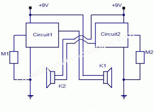
The circuit diagram represents a simple yet effective intercom system entirely based on transistors. It consists of three stages along with an RC amplifier. When the pushbutton S2 is pressed, the amplifier circuit around transistor T1 is activated. The intercom...
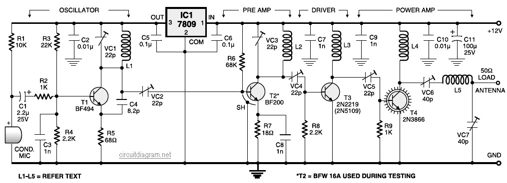
A four-stage FM transmitter circuit diagram utilizes four radio frequency stages: a VHF oscillator designed around the BF494 transistor (T1), a preamplifier based on the BF200 transistor (T2), a driver built with the 2N2219 transistor (T3), and a power...
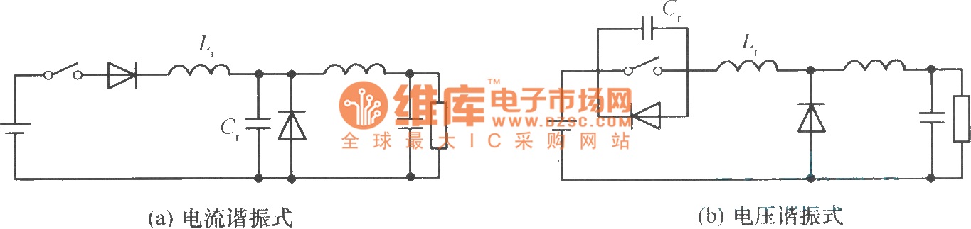
In a commonly used switching stabilized voltage supply, a resonant switch can be utilized to replace the shape of a step-down converter, resulting in a resonant converter circuit. The diagram illustrates the transformation from a step-down converter to a...
The alarm protection can trigger a sound and light alert when the mains voltage exceeds or falls below a predetermined threshold. It automatically disconnects the electrical power supply without damaging the electrical protection. The device is compact, fully featured,...
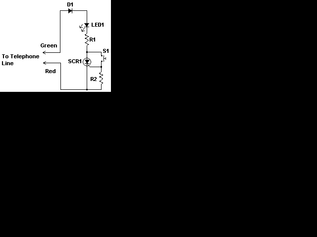
Although a hold feature is standard on most new phones, many users still utilize the original bell phones. For those who require a hold feature, this circuit is particularly useful. It is easy to construct and compact enough to...
An operational amplifier along with transistors Q1 and Q2 forms an exponential converter to produce an exponential gain control current, which is fed into the rectifier. A reference current of 150 pA, with a voltage of 15 V and...