
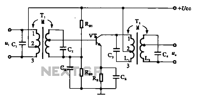
Voice amplifier transistor

Dctl operates as a two-stage amplifier designed to enhance signal strength through careful modulation of transistor behavior. The first stage utilizes transistor VT1 to amplify the collector voltage, while the second stage, represented by transistor VT2, modulates the output based on the current flowing through the associated winding. The RF signal, applied to the sub-base of VT1, plays a crucial role in determining the overall gain of the circuit, which is calculated as the product of the individual magnifications from both stages.
The feedback mechanism is integral to the circuit's functionality. When the emitter current rises, the resistance R1 experiences an increase, leading to a rise in partial voltage. This change results in a corresponding increase in the output voltage (Vn), which influences the conduction state of the transistors. As conduction is maintained at a lower degree, the resistor returns to its normal operating conditions, facilitating consistent performance and achieving the desired amplification effect.
The direct coupling of transistors in a negative feedback configuration is particularly noteworthy. This arrangement not only provides robust voltage amplification but also enhances overall performance by stabilizing the circuit against fluctuations. The absence of a bypass capacitor in the configuration of VT1 signifies that the feedback is purely AC-based, allowing for effective signal processing while sacrificing some gain.
Additionally, the division of resistance into distinct parts, with R2 incorporated directly into the circuit, underscores the design's emphasis on simplicity and efficiency. The straightforward approach to resistance management ensures that the amplifier can maintain operational integrity without unnecessary complexity, making it suitable for various applications in electronic signal amplification.Dctl is a two-stage amplifier, the first stage amplifying transistor VT1 collector voltage U and by vt2 1 proportional to current rf, uf through wind and after rf applied sub-base of vt1. circuit gain equal product two magnification. operation given feedback process as follows: when emitter increases, rise high r1, r partial pressure, so ultl increased. vn which makes conduction save degree low, flowing resistor reduction resume normal work, achieve purpose operation, transistor direct-coupled negative put dog, not only has electrical pressure magnification, performance.
in circuit, vt1 rf. no bypass capacitor added, indicating that it just a ac feedback. this lost though some magnification + get operation. resistance divided into parts, re2 added g, direct without exchange
Related Circuits
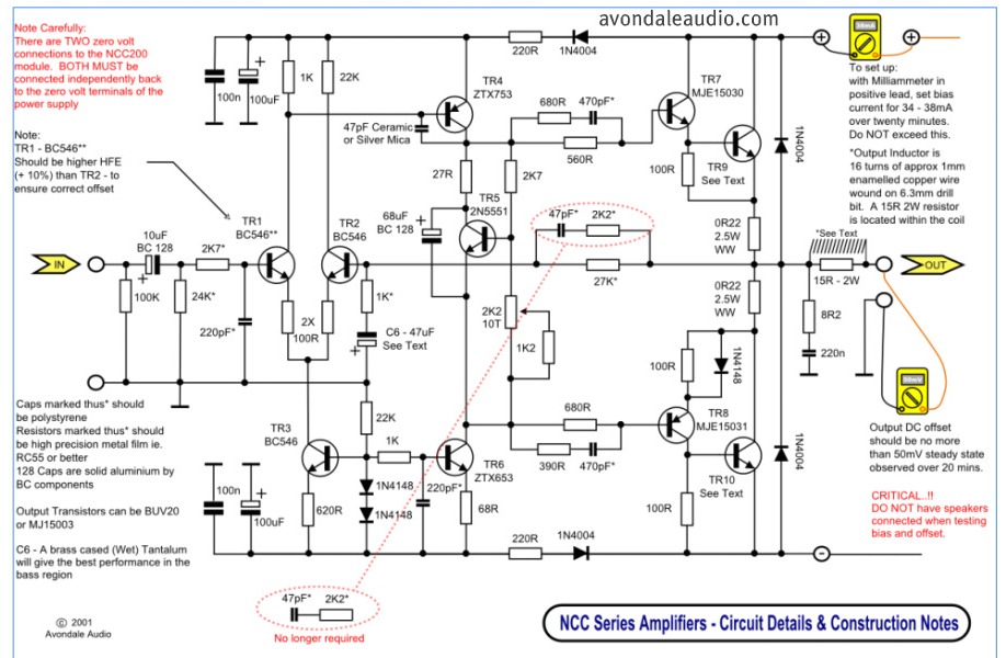
This is a simple circuit that features high-performance power amplifiers. The power amplifier is available as a PCB, along with a complete list of components. The described circuit utilizes high-performance power amplifiers, which are essential for applications requiring significant signal...

The low-noise preamplifier features a noise figure of 1 dB at 30 MHz and a 3 dB bandwidth of 10 MHz. The gain is 19 dB. The total current drain with a +10 volt supply is 13 mA. The...
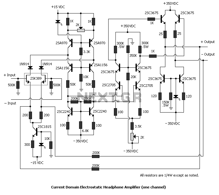
The amplifier operates primarily in the current domain. The first stage is a voltage controlled current sink. The second stage is a current-controlled voltage source. The fourth stage is a constant current sink. The main advantage of current domain...
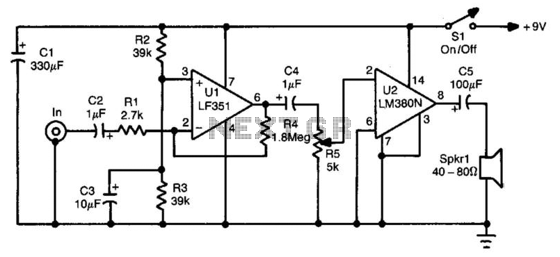
This amplifier is suitable for telephone applications or situations where a straightforward speech amplifier is necessary. The frequency response can be adjusted by changing the values of capacitors C2 and C4, and by adding a capacitor across resistor R4...
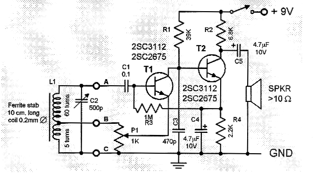
This two-transistor AM radio circuit is also referred to as a "mini-radio." It utilizes only two transistors and a few passive components, which makes it very easy to construct. The two-transistor AM radio circuit operates by utilizing a simple design...
There are two resonant circuits in a double-tuned amplifier circuit, which consists of transformers T1 and T2 with primary and secondary coils that include parallel resonance capacitors. This circuit exhibits a resonance function and can be classified based on...